TIDUEO0C July 2019 – March 2021
- Description
- Resources
- Features
- Applications
- 5
- 1System Description
-
2System Overview
- 2.1 Block Diagram
- 2.2 Design Considerations
- 2.3
Highlighted Products
- 2.3.1 TPS63900: 1.8V-5.5 VIN Buck-Boost Converter With 75-nA Ultra-low Quiescent Current and 400-mA Output Current
- 2.3.2 TPS610995: 0.7 VIN Synchronous Boost Converter With 400-nA Ultra-low Quiescent Current and 1-A Peak Current
- 2.3.3 TPS62840: 750-mA Synchronous Step-Down Converter With Ultra-low Quiescent Current Consumption
- 2.4 System Design Theory
- 3Hardware, Software, Testing Requirements, and Test Results
- 4Design Files
- 5Software Files
- 6Related Documentation
- 7Terminology
- 8About the Author
- 9Revision History
2.3.1 TPS63900: 1.8V-5.5 VIN Buck-Boost Converter With 75-nA Ultra-low Quiescent Current and 400-mA Output Current
The TPS63900 device is a high-efficiency (> 90% at 10-µA load current) synchronous buck-boost converter with an extremely low quiescent current (75 nA typical). The high efficiency over wide load ranges and a low IQ value helps prolong the battery life. With its wide supply voltage range and programmable input current limit (1 mA to 10 mA and unlimited), this device is ideal for use with a wide range of primary and secondary battery types such as 3S Alkaline, 1S Li-MnO2 or 1S Li-SOCl2.
A 2 level dynamic voltage-scaling feature lets applications switch between two output voltages during operation. DVS allows for optimizing output voltages for heavy and light load operation which reduces the total system power consumption. When the SEL pin changes state, the output voltage ramps to the new value in 100-mV steps. The duration of each step is 125 µs.
The TPS63900 uses a trapezoidal inductor current to regulate its output under all operating conditions. Thus, the device only has one operating mode and does not display any of the mode-change transients or unpredictable switching displayed by many other buck-boost devices. The switching frequency of the TPS63900 device varies with the operating conditions: it is lowest when output current is low and increases smoothly as output current increases.
The TPS63900 offers a wide array of safety and operation features. These include integrated soft start, output short circuit protection, and over temperature protection. The TPS63900 also features a programmable input current limit (1 mA to 100 mA and unlimited) to protect batteries that do not support high peak currents.
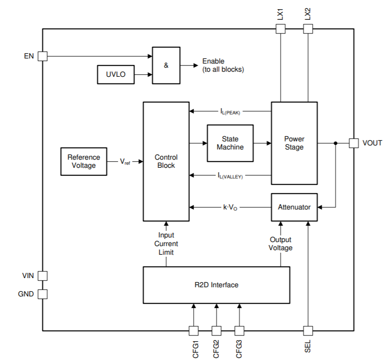
 Figure 2-2 TPS63900 Functional Block
Diagram.