TIDUEO0C July 2019 – March 2021
- Description
- Resources
- Features
- Applications
- 5
- 1System Description
-
2System Overview
- 2.1 Block Diagram
- 2.2 Design Considerations
- 2.3
Highlighted Products
- 2.3.1 TPS63900: 1.8V-5.5 VIN Buck-Boost Converter With 75-nA Ultra-low Quiescent Current and 400-mA Output Current
- 2.3.2 TPS610995: 0.7 VIN Synchronous Boost Converter With 400-nA Ultra-low Quiescent Current and 1-A Peak Current
- 2.3.3 TPS62840: 750-mA Synchronous Step-Down Converter With Ultra-low Quiescent Current Consumption
- 2.4 System Design Theory
- 3Hardware, Software, Testing Requirements, and Test Results
- 4Design Files
- 5Software Files
- 6Related Documentation
- 7Terminology
- 8About the Author
- 9Revision History
2.4.2.3 Current Ranges Simulation With TINA-TI
Figure 2-6 shows the TINA-TI simulation results with the current flowing through the 0.1-Ω resistance. When injecting a 493-mA current into the system, the input voltage of operational amplifier is 69.03 mV (slightly above the calculated 69 mV). The resulting output voltage is 3.29 V, which is close to the calculations in Section 2.4.2.2 and the 3.3 V full-scale voltage.
 Figure 2-6 TINA-TI Simulation for the High-Current Range Using 0.1-Ω Resistor Value
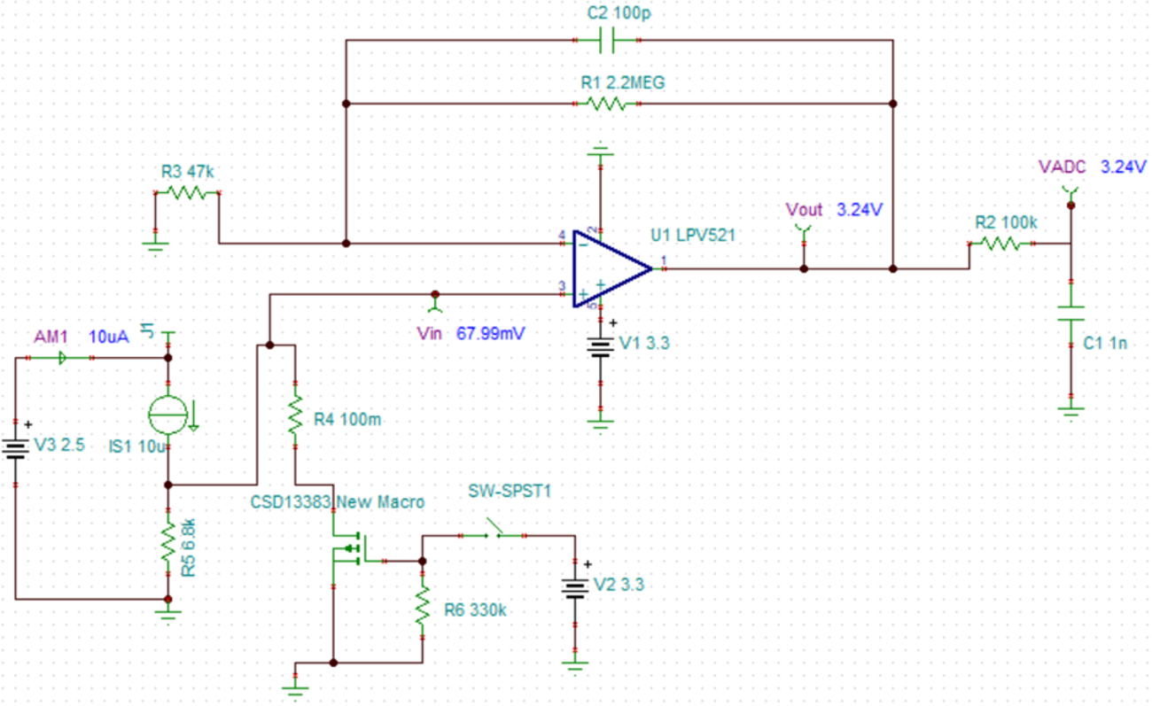
Figure 2-7 shows the simulation of the current flowing through the 6.8-kΩ resistor. With 10-µA current into the system, the input voltage of the LPV521 device is 67.99 mV (a bit below the 69 mV maximum value).
 Figure 2-7 TINA-TI Simulation for the Low-Current Range Using 6.8-kΩ Resistor Value
The simulated output voltage is 3.24 V, also slightly below the maximum allowed voltage of 3.3 V, which is in line with the calculated results.
Using the TINA-TI simulation file included with this reference design, designers can calculate the resistor values required for their application.