TIDUEY6 April 2021
- Description
- Resources
- Features
- Applications
- 5
- 1System Description
- 2System Overview
-
3Hardware, Software, Testing Requirements, and Test Results
- 3.1
Hardware Requirements
- 3.1.1
Hardware Overview
- 3.1.1.1
Control Module
- 3.1.1.1.1
Control Mother Board
- 3.1.1.1.1.1 Inverter Safing - UCC5870 ASC and Fault Control
- 3.1.1.1.1.2 DC-DC Safing
- 3.1.1.1.1.3 DC-DC Converter Secondary PWM Selection
- 3.1.1.1.1.4 Blower Fan Control
- 3.1.1.1.1.5 Voltage Monitor
- 3.1.1.1.1.6 Resolver Interface Control
- 3.1.1.1.1.7 Test Points on Control Module
- 3.1.1.1.1.8 General Purpose Ports
- 3.1.1.1.1.9 Connectors and Headers on Control Mother Board
- 3.1.1.1.2 Power Supplies
- 3.1.1.1.3 TCAN4550 module
- 3.1.1.1.4 Dual TCAN Module
- 3.1.1.1.5 Analog Back End Module
- 3.1.1.1.6 Resolver Analog Front End Module
- 3.1.1.1.1
Control Mother Board
- 3.1.1.2 Inverter Module
- 3.1.1.3 DC-DC Bidirectional Converter Module
- 3.1.1.1
Control Module
- 3.1.1
Hardware Overview
- 3.2 Resource Mapping
- 3.3 Test Setup
- 3.4 Test Results
- 3.1
Hardware Requirements
- 4General Texas Instruments High Voltage Evaluation (TI HV EVM) User Safety Guidelines
- 5Design and Documentation Support
- 6About the Author
3.1.1.1.2.3 Power Supply 15-V/0.5-A
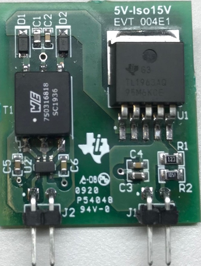
This is another compact power module based on SN6501-Q1 and TL1963A-Q1. The design is based off Signal and power isolation with 3.3 V / 5 V input and 12 V / 15 V output. Design information is available in this user guide. The layout of this module is customized to fit the requirements of this EV traction reference design and is shown in Figure 3-14.
 Figure 3-14 5-V to
15-V/0.5-A power supply module
Figure 3-14 5-V to
15-V/0.5-A power supply moduleThis module is fed by the intermediate 5-V power supply and its output will power the resolver module. This module will mount on control mother board connectors J31 and J32 and its component side will face the resolver module connector J9 on mother board.