TIDUEY6 April 2021
- Description
- Resources
- Features
- Applications
- 5
- 1System Description
- 2System Overview
-
3Hardware, Software, Testing Requirements, and Test Results
- 3.1
Hardware Requirements
- 3.1.1
Hardware Overview
- 3.1.1.1
Control Module
- 3.1.1.1.1
Control Mother Board
- 3.1.1.1.1.1 Inverter Safing - UCC5870 ASC and Fault Control
- 3.1.1.1.1.2 DC-DC Safing
- 3.1.1.1.1.3 DC-DC Converter Secondary PWM Selection
- 3.1.1.1.1.4 Blower Fan Control
- 3.1.1.1.1.5 Voltage Monitor
- 3.1.1.1.1.6 Resolver Interface Control
- 3.1.1.1.1.7 Test Points on Control Module
- 3.1.1.1.1.8 General Purpose Ports
- 3.1.1.1.1.9 Connectors and Headers on Control Mother Board
- 3.1.1.1.2 Power Supplies
- 3.1.1.1.3 TCAN4550 module
- 3.1.1.1.4 Dual TCAN Module
- 3.1.1.1.5 Analog Back End Module
- 3.1.1.1.6 Resolver Analog Front End Module
- 3.1.1.1.1
Control Mother Board
- 3.1.1.2 Inverter Module
- 3.1.1.3 DC-DC Bidirectional Converter Module
- 3.1.1.1
Control Module
- 3.1.1
Hardware Overview
- 3.2 Resource Mapping
- 3.3 Test Setup
- 3.4 Test Results
- 3.1
Hardware Requirements
- 4General Texas Instruments High Voltage Evaluation (TI HV EVM) User Safety Guidelines
- 5Design and Documentation Support
- 6About the Author
3.1.1.2.3 Inverter Current Sense Module
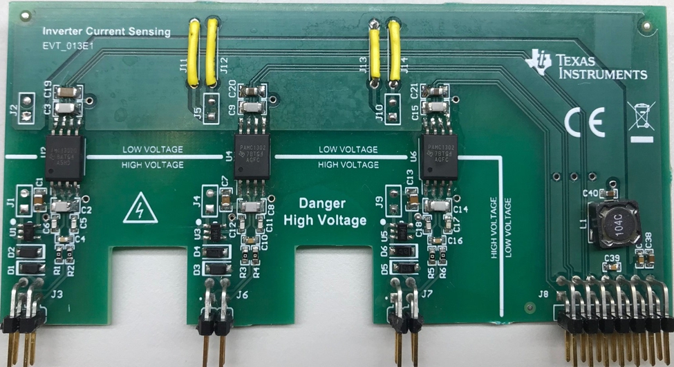
Current sense module is designed to provide isolated differential analog feedback of inverter phase currents. This is designed using isolation amplifier AMC1302-Q1 and is based on AMC130x Evaluation Module. A picture of this board is shown in Figure 3-24.
 Figure 3-24 Inverter Current Sense Board
AMC1302 measures phase current by measuring voltage drop across a shunt resistor. Since its designed input voltage range is ±50mV, a low value shunt resistor is only needed thereby leading to a lower power dissipation. It has a fixed gain with low drift: 41 ± 0.3%, ±50 ppm/°C, low input offset and drift of, low non-linearity and drift, output bandwidth above 200KHz and a rise time/fall time of sub 2μs. All these features make it suitable for this application.
AMC1302 will require separate power supplies for the high voltage (HOT) and low voltage (COLD) sides. Isolated power supply for the HOT side of AMC1302 for each phase is derived from that phase's high side gate drive's secondary power supply (AH, BH, CH) and drop regulated to 3.3 V. Alternately, using the intermediate 5 V power supply routed to this board via J8, supplementary 5 V to 5 V isolated modules can be mounted on its headers J1, and J2, J4 and J5 and J9 and J10 for phases A, B and C respectively. COLD side power supply is provided from control mother board on a 8x2 header. This module is mounted on headers J5, J8, J11 and J16 of the inverter mother board. Feedback signals are brought out to 8x2 connector J16 of the inverter mother board.
| Header | Description |
|---|---|
| J1, J2 | Backup 5 V to Iso 5 V module for phase A hot current sensing side |
| J4, J5 | Backup 5 V to Iso 5 V module for phase B hot current sensing side |
| J9, J10 | Backup 5 V to Iso 5V module for phase C hot current sensing side |