TIDUEY6 April 2021
- Description
- Resources
- Features
- Applications
- 5
- 1System Description
- 2System Overview
-
3Hardware, Software, Testing Requirements, and Test Results
- 3.1
Hardware Requirements
- 3.1.1
Hardware Overview
- 3.1.1.1
Control Module
- 3.1.1.1.1
Control Mother Board
- 3.1.1.1.1.1 Inverter Safing - UCC5870 ASC and Fault Control
- 3.1.1.1.1.2 DC-DC Safing
- 3.1.1.1.1.3 DC-DC Converter Secondary PWM Selection
- 3.1.1.1.1.4 Blower Fan Control
- 3.1.1.1.1.5 Voltage Monitor
- 3.1.1.1.1.6 Resolver Interface Control
- 3.1.1.1.1.7 Test Points on Control Module
- 3.1.1.1.1.8 General Purpose Ports
- 3.1.1.1.1.9 Connectors and Headers on Control Mother Board
- 3.1.1.1.2 Power Supplies
- 3.1.1.1.3 TCAN4550 module
- 3.1.1.1.4 Dual TCAN Module
- 3.1.1.1.5 Analog Back End Module
- 3.1.1.1.6 Resolver Analog Front End Module
- 3.1.1.1.1
Control Mother Board
- 3.1.1.2 Inverter Module
- 3.1.1.3 DC-DC Bidirectional Converter Module
- 3.1.1.1
Control Module
- 3.1.1
Hardware Overview
- 3.2 Resource Mapping
- 3.3 Test Setup
- 3.4 Test Results
- 3.1
Hardware Requirements
- 4General Texas Instruments High Voltage Evaluation (TI HV EVM) User Safety Guidelines
- 5Design and Documentation Support
- 6About the Author
3.1.1.3 DC-DC Bidirectional Converter Module
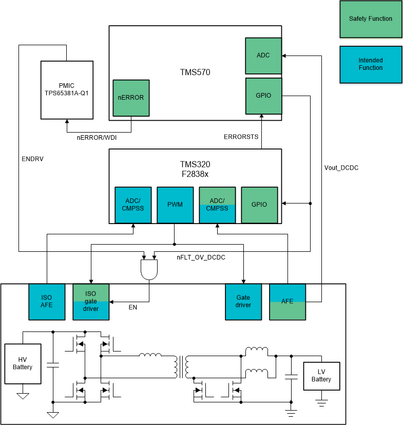
The bi-directional DC-DC converter module is designed to charge the LV battery from HV battery bus when operate in forward direction and per-charge the DC bus capacitor in reverse direction. It is a separate module that plugs into control mother board to receive control power and signals and to send back inverter voltage and current sense signals as feedback. It consists of a main board and two gate driver daughter boards for isolated primary gate driver and power supply.
A block diagram of the traction inverter sub-system is shown in Figure 3-26.
 Figure 3-26 DC-DC System Block Diagram
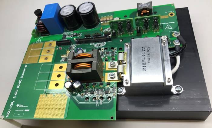
A fully assembled picture of inverter module is shown in Figure 3-27. Details of various sub-modules will be discussed in subsequent sections.
 Figure 3-27 DC-DC Converter Module