TIDUEY6 April 2021
- Description
- Resources
- Features
- Applications
- 5
- 1System Description
- 2System Overview
-
3Hardware, Software, Testing Requirements, and Test Results
- 3.1
Hardware Requirements
- 3.1.1
Hardware Overview
- 3.1.1.1
Control Module
- 3.1.1.1.1
Control Mother Board
- 3.1.1.1.1.1 Inverter Safing - UCC5870 ASC and Fault Control
- 3.1.1.1.1.2 DC-DC Safing
- 3.1.1.1.1.3 DC-DC Converter Secondary PWM Selection
- 3.1.1.1.1.4 Blower Fan Control
- 3.1.1.1.1.5 Voltage Monitor
- 3.1.1.1.1.6 Resolver Interface Control
- 3.1.1.1.1.7 Test Points on Control Module
- 3.1.1.1.1.8 General Purpose Ports
- 3.1.1.1.1.9 Connectors and Headers on Control Mother Board
- 3.1.1.1.2 Power Supplies
- 3.1.1.1.3 TCAN4550 module
- 3.1.1.1.4 Dual TCAN Module
- 3.1.1.1.5 Analog Back End Module
- 3.1.1.1.6 Resolver Analog Front End Module
- 3.1.1.1.1
Control Mother Board
- 3.1.1.2 Inverter Module
- 3.1.1.3 DC-DC Bidirectional Converter Module
- 3.1.1.1
Control Module
- 3.1.1
Hardware Overview
- 3.2 Resource Mapping
- 3.3 Test Setup
- 3.4 Test Results
- 3.1
Hardware Requirements
- 4General Texas Instruments High Voltage Evaluation (TI HV EVM) User Safety Guidelines
- 5Design and Documentation Support
- 6About the Author
3.1.1.1.6 Resolver Analog Front End Module
Resolver analog front end module deals with all the analog interface requirements of the resolver to work with MCUs. It has two main functions:
- Excitation signal amplification: This module filters the sinusoidal signal generated from MCU via DAC or PWM interface into a smooth sinusoidal excitation carrier signal and amplifies it into appropriate voltage and power level to feed the excitation winding of resolver.
- Feedback signal conditioning: the bipolar sine and cosine outputs of the resolver into unipolar signals to fit within ADC measurement range of MCUs
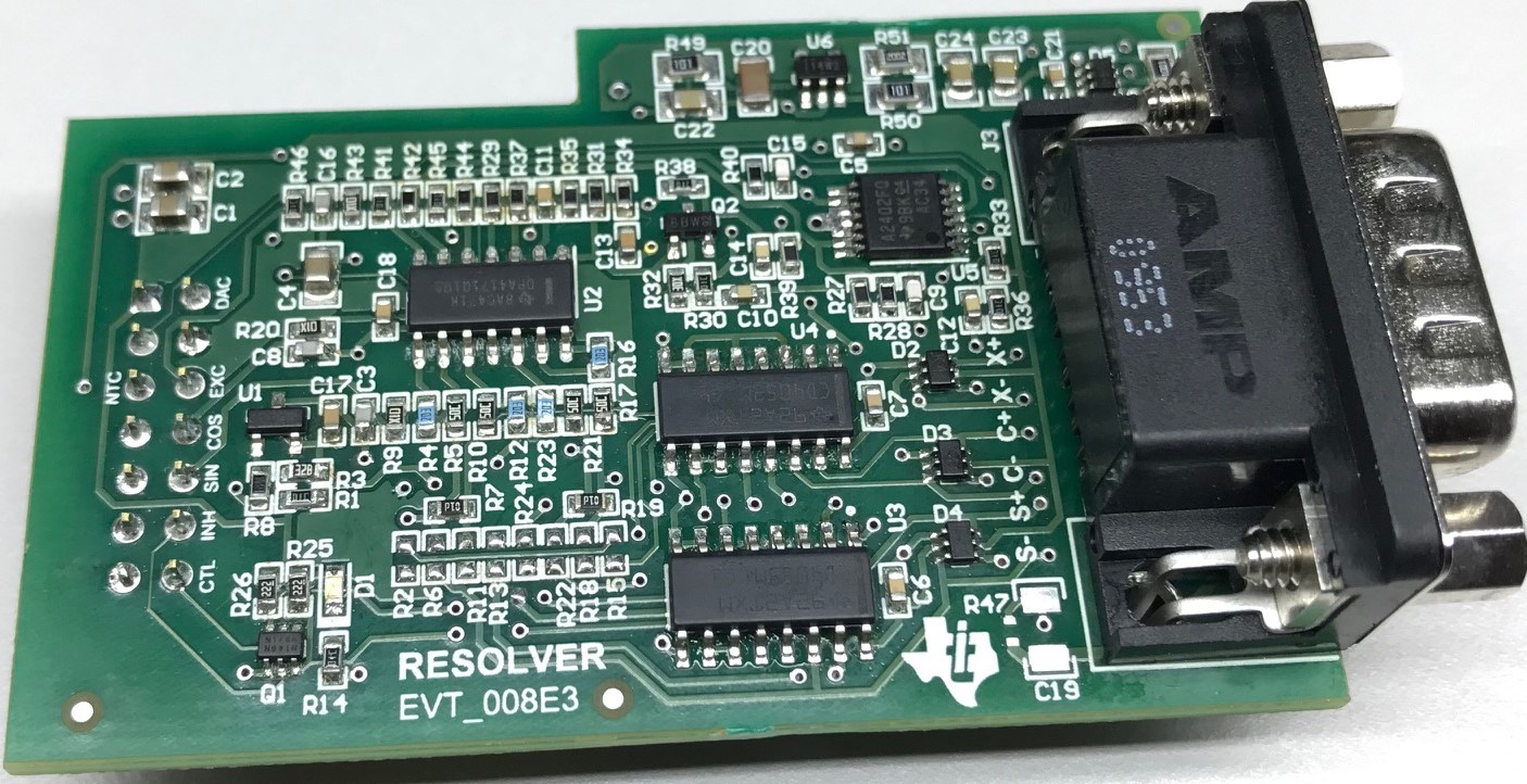
The module is designed using ALM2402F-Q1 and standard linear parts. ALM2402F-Q1 is a dual channel high power operational amplifier with integrated protection for resolver against current limit and over temperature. The module is shown in Figure 3-18.
 Figure 3-18 Resolver Analog Front End
Module
Figure 3-18 Resolver Analog Front End
ModuleIt is mounted on control mother board headers J8, J9 and J10. All power and signals are flow through J9, while J10 provides EARTH access to noise signals picked by resolver cable. J8 provides mechanical support for the module. The module has a multiplexer CD4053B-Q1 that helps to cross feed the sine and cosine signals into ADC to verify signal and channel integrity to ensure safe estimation of rotor position. The module also interfaces with resolver thermistor and provides an analog signal representing resolver temperature for the MCUs to track.