TIDUEY6 April 2021
- Description
- Resources
- Features
- Applications
- 5
- 1System Description
- 2System Overview
-
3Hardware, Software, Testing Requirements, and Test Results
- 3.1
Hardware Requirements
- 3.1.1
Hardware Overview
- 3.1.1.1
Control Module
- 3.1.1.1.1
Control Mother Board
- 3.1.1.1.1.1 Inverter Safing - UCC5870 ASC and Fault Control
- 3.1.1.1.1.2 DC-DC Safing
- 3.1.1.1.1.3 DC-DC Converter Secondary PWM Selection
- 3.1.1.1.1.4 Blower Fan Control
- 3.1.1.1.1.5 Voltage Monitor
- 3.1.1.1.1.6 Resolver Interface Control
- 3.1.1.1.1.7 Test Points on Control Module
- 3.1.1.1.1.8 General Purpose Ports
- 3.1.1.1.1.9 Connectors and Headers on Control Mother Board
- 3.1.1.1.2 Power Supplies
- 3.1.1.1.3 TCAN4550 module
- 3.1.1.1.4 Dual TCAN Module
- 3.1.1.1.5 Analog Back End Module
- 3.1.1.1.6 Resolver Analog Front End Module
- 3.1.1.1.1
Control Mother Board
- 3.1.1.2 Inverter Module
- 3.1.1.3 DC-DC Bidirectional Converter Module
- 3.1.1.1
Control Module
- 3.1.1
Hardware Overview
- 3.2 Resource Mapping
- 3.3 Test Setup
- 3.4 Test Results
- 3.1
Hardware Requirements
- 4General Texas Instruments High Voltage Evaluation (TI HV EVM) User Safety Guidelines
- 5Design and Documentation Support
- 6About the Author
3.1.1.1.1.1 Inverter Safing - UCC5870 ASC and Fault Control
Safe operation of traction inverter for the assumed safety goals is critical to system level ASIL-D compliance. Over current protection is handled by CMPSS of the C2000 device. This is a software programmable limit. There is also a redundant hardware detection for over current for a certain absolute maximum limit of the inverter. In the event of these hardware not able to detect the over current limits in a timely manner, such as a short circuit, a quick response is needed to protect the inverter. UCC5870 is an ASIL-D compliant gate driver with many features.
For active short circuit (ASC) protection, it gives the user a choice to configure the logic state of the driver if such an event is detected. For example, the user could shut down all switches or shut down only the bottom switches or top switches. In this reference design, there are two MCUs each having a certain level of functional safety requirement. During development and testing, there should be an option to set these up by either safety MCU or control MCU or be put in a default setting.
In the first stage, an arbitration between being set by safety MCU and default hard settings is chosen with a multiplexer. Default setting is done using resistors connected to XX_IN pins of CD4053 MUX and is shown in Figure 3-3. These resistors can be tied to one of the power rails to set the desired logic level. Selection between these two signal sources (Safety MCU vs default settings) is done by EN_DRV signal that is generated by a PMIC device on safety MCU control card. If EN_DRV is activated, then the hard choices chosen by default resistor settings will be chosen for ASC otherwise the settings provided safety MCU will be chosen.
 Figure 3-3 ASC Logic Selection between Safety MCU and
Default Setting
Figure 3-3 ASC Logic Selection between Safety MCU and
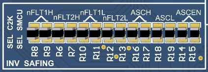
Default SettingIn the second stage, a further arbitration is done between the output of first stage and that of the C2000MCU. This is done using 0E resistors that will act as a switch. These will connect the arbitration stage outputs and UCC5870 gate drivers. Besides the ASC signals, there nFLTx_y signals that represent the primary and secondary side faults of low side and high side gate drivers. These are linked to either the safety MCU or C2000 MCU through a bunch of 0E resistors that are present alongside that of ASC second stage arbitration 0E resistors as shown in Figure 3-4. Populating resistors on the left side will select C2000 MCU and that on the right will select Safety MCU.
 Figure 3-4 Selection Between C2000 and Safety MCUs
to Connect ASC and nFLT
Figure 3-4 Selection Between C2000 and Safety MCUs
to Connect ASC and nFLTDO NOT populate both resistors of ASCx selection with an intent to connect to both MCUs. Since the ASC signals are either tied to power rails or digital outputs driven by respective MCUs, connecting them together can damage the GPIOs that are at different logic levels.
nFLTxy signals are inputs to MCUs and hence it is OK to populate both resistors to connect with both MCUs.