Packaging information
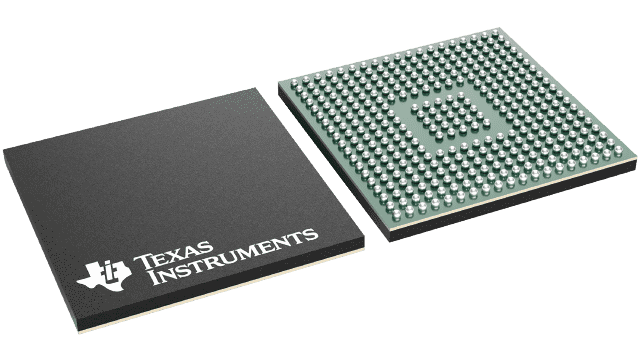
| Package | Pins NFBGA (GWT) | 337 |
| Operating temperature range (°C) -55 to 125 |
| Package qty | Carrier 90 | JEDEC TRAY (5+1) |
Features for the TMS570LS20216-EP
- The TMS570LS20206-EP and TMS570LS20216-EP use the same silicon (die) as the TMS
TMS570LS Series IEC 61508 SIL3 certified microcontroller family however it is instead
certified to meet GEIA-STD-00021-1 for Aerospace Qualified Electronic Components
and tested for operation over the military temperature range. - High-Performance Microcontroller
- Dual CPUs running in Lockstep
- ECC on Flash and SRAM
- CPU and Memory BIST (Built-In Self Test)
- Error Signaling Module (ESM) w/ Error Pin
- ARM® Cortex™-R4F 32-Bit RISC CPU
- Efficient 1.6 DMIPS/MHz with 8-stage pipeline
- Floating Point Unit with Single/Double Precision
- Memory Protection Unit (MPU)
- Open Architecture With Third-Party Support
- Operating Features
- Up to 160-MHz System Clock
- Core Supply Voltage (VCC): 1.5 V
- I/O Supply Voltage (VCCIO): 3.3 V
- Integrated Memory
- 2M-Byte Flash with ECC
- 60K-Byte RAM with ECC
- Multiple Communication interfaces including FlexRay, CAN, and LIN
- NHET Timer and 2x 12-bit ADCs
- External Memory Interface (EMIF)
- 16bit Data, 22bit Address, 4 Chip Selects
- Common TMS570 Platform Architecture
- Consistent Memory Map across the family
- Real-Time Interrupt (RTI) OS Timer
- Vectored Interrupt Module (VIM)
- Cyclic Redundancy Checker (CRC,
2 Channels)
- Direct Memory Access (DMA) Controller
- 32 DMA requests and 16 Channels/ Control Packets
- Parity on Control Packet Memory
- Dedicated Memory Protection Unit (MPU)
- Frequency-Modulated Zero-Pin Phase-Locked Loop (FMzPLL)-Based Clock Module
- Oscillator and PLL clock monitor
- Up to 115 Peripheral IO pins
- 16 Dedicated GIO - 8 w/ External Interrupts
- Programmable External Clock (ECLK)
- Communication Interfaces
- Three Multi-buffered Serial Peripheral Interface (MibSPI) each
with:Four Chip Selects and one Enable pin128 buffers with parityOne with
parallel mode - Two UART (SCI) interfaces with Local Interconnect Network Interface (LIN 2.0)
- Three CAN (DCAN) ControllerTwo with 64 mailboxes, one with 32Parity on mailbox RAM
- Dual Channel FlexRay™ Controller8K-Byte message RAM with parityTransfer Unit
with MPU and parity
- Three Multi-buffered Serial Peripheral Interface (MibSPI) each
- High-End Timer (NHET)
- 32 Programmable I/O Channels
- 128 Words High-End Timer RAM with parity
- Transfer Unit with MPU and parity
- Two 12-Bit Multi-Buffered ADCs (MibADC)
- 24 total ADC Input channels
- Each has 64 Buffers with parity
- Trace and Calibration Interfaces
- Embedded Trace Module (ETMR4)
- Data Modification Module (DMM)
- RAM Trace Port (RTP)
- Parameter Overlay Module (POM)
- On-Chip emulation logic including IEEE 1149.1 JTAG, Boundary Scan and
ARM Coresight components - Full Development Kit Available
- Development Boards
- Code Composer Studio Integrated Development Environment (IDE)
- HaLCoGen Code Generation Tool
- HET Assembler and Simulator
- nowFlash Flash Programming Tool
- Packages Supported
- 337-Pin Ball Grid Array (GWT)
- 144-Pin Lidded Quad Flat Pack (PGE)
- Community Resources
SUPPORTS DEFENSE AND AEROSPACE APPLICATIONS
- Controlled Baseline
- One Assembly/Test Site
- One Fabrication Site
- Rated From –55°C to 125°C
- Extended Product Life Cycle
- Extended Product-Change Notification
- Product Traceability
Description for the TMS570LS20216-EP
The TMS570LS series is a high performance microcontroller family. The architecture includes Dual CPUs in lockstep, CPU and Memory Built-In Self Test (BIST) logic, ECC on both the Flash and the data SRAM, parity on peripheral memories, and loop back capability on peripheral IOs.
The TMS570LS family integrates the ARM® Cortex™-R4F Floating Point CPU which offers an efficient 1.6 DMIPS/MHz, and has configurations which can run up to 160 MHz providing more than 250 DMIPS. The TMS570LS series also provides Flash (2MB) and data SRAM (160KB) options with single bit error correction and double bit error detection.
The TMS570LS devices feature peripherals for real-time control-based applications, including up to 32 nHET timer channels and two 12-bit A to D converters supporting up to 24 inputs. There are multiple communication interfaces including a 2-channel FlexRay, 3 CAN controllers supporting 64 mailboxes each, and 2 LIN/UART controllers.
With a wide choice of communication and control peripherals, the TMS570LS series is an ideal solution for high performance real time control applications.
The devices included in the TMS570LS series and described in this document are:
- TMS570LS20206
- TMS570LS20216
The TMS570LS series microcontrollers contain the following:
- Dual TMS570 16/32-Bit RISC (ARM Cortex™-R4F) in Lockstep
- Up to 2M-Byte Program Flash with ECC
- Up to 160K-Byte Static RAM (SRAM) with ECC
- Real-Time Interrupt (RTI) Operating System Timer
- Vectored Interrupt Module (VIM)
- Cyclic Redundancy Checker (CRC) with Parallel Signature Analysis (PSA)
- Direct Memory Access (DMA)Controller
- Frequency-Modulated Phase-Locked Loop (FMzPLL)-Based Clock Module With Prescaler
- Three Multi-buffered Serial Peripheral Interfaces (MibSPI)
- Two UARTs (SCI) with Local Interconnect Network Interfaces (LIN)
- Three CAN Controllers (DCAN)
- High-End Timer (NHET) with dedicated Transfer Unit (HTU)
- Available FlexRay Controller with dedicated PLL and Transfer Unit (FTU)
- External Clock Prescale (ECP) Module
- Two 16-Channel 12-Bit Multi-Buffered ADCs (MibADC) - 8 shared channels between the two ADCs
- Address Bus Parity with Failure Detection
- Error Signaling Module (ESM) with external error pin
- Voltage Monitor (VMON) with out of range reset assertion
- Embedded Trace Module (ETMR4)
- Data Modification Module (DMM)
- RAM Trace Port (RTP)
- Parameter Overlay Module (POM)
- 16 Dedicated General-Purpose I/O (GIO) Pins for GWT; 8 Dedicated GIO Pins for PGE
- 115 Total Peripheral I/Os for GWT; 68 Total Peripheral I/Os for PGE
- 16-Bit External Memory Interface (EMIF)
The devices utilize the big-endian format where the most significant byte of a word is stored at the lowest numbered byte and the least significant byte at the highest numbered byte.
The device memory includes general-purpose SRAM supporting single-cycle read/write accesses in byte, halfword, and word modes. The flash memory on this device is a nonvolatile, electrically erasable and programmable memory implemented with a 64-bit-wide data bus interface. The flash operates on a 3.3V supply input (same level as I/O supply) for all read, program and erase operations. When in pipeline mode, the flash operates with a system clock frequency of up to 160 MHz.
The device has nine communication interfaces: three MibSPIs, two LIN/SCIs, three DCANs and one FlexRay™ controller (optional). The SPI provides a convenient method of serial interaction for high-speed communications between similar shift-register type devices. The LIN supports the Local Interconnect standard 2.0 and can be used as a UART in full-duplex mode using the standard Non-Return-to-Zero (NRZ) format. The DCAN supports the CAN 2.0B protocol standard and uses a serial, multimaster communication protocol that efficiently supports distributed real-time control with robust communication rates of up to 1 megabit per second (Mbps). The DCAN is ideal for applications operating in noisy and harsh environments that require reliable serial communication or multiplexed wiring. The FlexRay uses a dual channel serial, fixed time base multimaster communication protocol with communication rates of 10 megabits per second (Mbps) per channel. A FlexRay Transfer Unit (FTU) enables autonomous transfers of FlexRay data to and from main CPU memory. Transfers are protected by a dedicated, built-in Memory Protection Unit (MPU).
The NHET is an advanced intelligent timer that provides sophisticated timing functions for real-time applications. The timer is software-controlled, using a reduced instruction set, with a specialized timer micromachine and an attached I/O port. The NHET can be used for pulse width modulated outputs, capture or compare inputs, or general-purpose I/O. It is especially well suited for applications requiring multiple sensor information and drive actuators with complex and accurate time pulses. A High End Timer Transfer Unit (HET-TU) provides features to transfer NHET data to or from main memory. A Memory Protection Unit (MPU) is built into the HET-TU to protect against erroneous transfers.
The device has two 12-bit-resolution MibADCs with 24 total channels and 64 words of parity protected buffer RAM each. The MibADC channels can be converted individually or can be grouped by software for sequential conversion sequences. Eight channels are shared between the two ADCs. There are three separate groupings, two of which are triggerable by an external event. Each sequence can be converted once when triggered or configured for continuous conversion mode.
The frequency-modulated phase-locked loop (FMzPLL) clock module contains a phase-locked loop, a clock-monitor circuit, a clock-enable circuit, and a prescaler. The function of the FMzPLL is to multiply the external frequency reference to a higher frequency for internal use. The FMzPLL provides one of the six possible clock source inputs to the global clock module (GCM). The GCM module provides system clock (HCLK), real-time interrupt clock (RTICLK1), CPU clock (GCLK), NHET clock (VCLK2), DCAN clock (AVCLK1), and peripheral interface clock (VCLK) to all other peripheral modules.
The device also has an external clock prescaler (ECP) module that when enabled, outputs a continuous external clock on the ECLK pin. The ECLK frequency is a user-programmable ratio of the peripheral interface clock (VCLK) frequency.
The Direct Memory Access Controller (DMA) has 32 DMA requests, 16 Channels/ Control Packets and parity protection on its memory. The DMA provides memory to memory transfer capabilities without CPU interaction. A Memory Protection Unit (MPU) is built into the DMA to protect memory against erroneous transfers.
The Error Signaling Module (ESM) monitors all device errors and determines whether an interrupt or external Error pin is triggered when a fault is detected.
The External Memory Interface (EMIF) provides a memory extension to asynchronous memories or other slave devices.
Several interfaces are implemented to enhance the debugging capabilities of application code. In addition to the built in ARM Cortex™-R4F CoreSight™ debug features, an External Trace Macrocell (ETM) provides instruction and data trace of program execution. For instrumentation purposes, a RAM Trace Port Module (RTP) is implemented to support high-speed output of RAM accesses by the CPU or any other master. A Direct Memory Module (DMM) gives the ability to write external data into the device memory. Both the RTP and DMM have no or only minimum impact on the program execution time of the application code. A Parameter Overlay Module (POM) can re-route Flash accesses to the EMIF, thus avoiding the re-programming steps necessary for parameter updates in Flash.