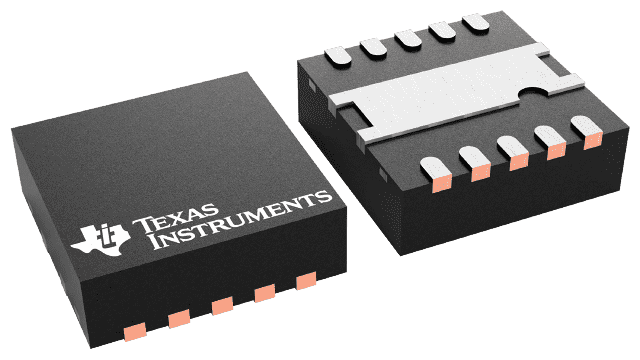
Packaging information
| Package | Pins VSON (DRC) | 10 |
| Operating temperature range (°C) -40 to 85 |
| Package qty | Carrier 250 | SMALL T&R |
Features for the ADS8867
- Sample Rate: 100 kHz
- No Latency Output
- Unipolar, True-Differential Input Range:
–VREF to +VREF - Wide Common-Mode Voltage Range:
0 V to VREF with 90-dB CMRR (min) - SPI™-Compatible Serial Interface with
Daisy-Chain Option - Excellent AC and DC Performance:
- SNR: 96 dB, THD: –115 dB
- INL: ±1.0 LSB (max)
- DNL: ±1.0 LSB (max), 16-Bit NMC
- Wide Operating Range:
- AVDD: 2.7 V to 3.6 V
- DVDD: 1.65 V to 3.6 V
(Independent of AVDD) - REF: 2.5 V to 5 V (Independent of AVDD)
- Operating Temperature: –40°C to +85°C
- Low-Power Dissipation:
- 0.7 mW at 100 kSPS
- 70 µW at 10 kSPS
- Power-Down Current (AVDD): 50 nA
- Full-Scale Step Settling to 16 Bits: 1200 ns
- Packages: MSOP-10 and SON-10
Description for the ADS8867
The ADS8867 is a 16-bit, 100-kSPS, true-differential input, analog-to-digital converter (ADC). The device operates with a 2.5-V to 5-V external reference, offering a wide selection of signal ranges without additional input signal scaling. The reference voltage setting is independent of, and can exceed, the analog supply voltage (AVDD).
The device offers an SPI-compatible serial interface that also supports daisy-chain operation for cascading multiple devices.
The device supports unipolar, true-differential analog input signals with a differential input swing of –VREF to +VREF. This true-differential analog input structure allows for a common-mode voltage of any value in the range of 0 V to +VREF (when both inputs are within the operating input range of –0.1 V to VREF + 0.1 V).
Device operation is optimized for very low-power operation. Power consumption directly scales with speed. This feature makes the ADS8867 excellent for lower-speed applications.