SBOS671D September 2018 – December 2022 OPA2828 , OPA828
PRODUCTION DATA
- 1 Features
- 2 Applications
- 3 Description
- 4 Revision History
- 5 Pin Configuration and Functions
- 6 Specifications
-
7 Detailed Description
- 7.1 Overview
- 7.2 Functional Block Diagram
- 7.3
Feature Description
- 7.3.1 Phase-Reversal Protection
- 7.3.2 Electrical Overstress
- 7.3.3 MUX Friendly Inputs
- 7.3.4 Overload Power Limiter
- 7.3.5 Noise Performance
- 7.3.6 Capacitive Load and Stability
- 7.3.7 Settling Time
- 7.3.8 Slew Rate
- 7.3.9 Full-Power Bandwidth
- 7.3.10 Small-Signal Response
- 7.3.11 Thermal Shutdown
- 7.3.12 Low Offset Voltage Drift
- 7.3.13 Overload Recovery
- 7.4 Device Functional Modes
- 8 Application and Implementation
- 9 Device and Documentation Support
- 10Mechanical, Packaging, and Orderable Information
Package Options
Mechanical Data (Package|Pins)
Thermal pad, mechanical data (Package|Pins)
- DGN|8
Orderable Information
7.3.2 Electrical Overstress
The OPAx828 are internally protected against electrostatic discharge (ESD) events that can occur during manufacturing, handling, or printed-circuit-board (PCB) assembly. The internal ESD protection diodes are not intended to protect the OPAx828 during normal operation when the devices are operating under power. The ESD protection circuitry involves several current-steering diodes connected from the input and output pins and routed back to the internal power-supply lines, where the diodes meet at the power-supply ESD cell, an absorption device, internal to the operational amplifiers. This protection circuitry is intended to remain inactive during normal circuit operation. In cases where the inputs or output can be driven above the positive power supply or below the negative power supply, make sure to limit the current through the internal diodes to 10 mA or less. In harsh electrical environments, external protection circuitry can be required depending on the application requirements and environmental conditions.
 Figure 7-2 Equivalent
Internal ESD Circuitry
Figure 7-2 Equivalent
Internal ESD CircuitryFigure 7-3 illustrates one example of protecting the OPAx828 inputs against an input overvoltage condition. In this example, the noninverting inputs to the OPAx828 are protected with the addition of an external resistor. If the input voltage, VIN, exceeds either power supply voltage, the input ESD diodes become forward biased at approximately 0.5 V. Limit the current through the forward-biased internal ESD diodes under such conditions; see Section 6.1. Figure 7-3 illustrates a specific example where the addition of the input resistor provides the necessary current limiting and allows for input voltages at VIN up to ±25.5 V. Assuming a symmetrical, dual power-supply configuration, the maximum input voltage for this circuit configuration can be determined from the following equation:
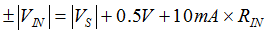
 Figure 7-3 Limiting the Input Current
Adding a series input protection resistor adds an additional source of noise to the circuit. Resistance values less than 250 Ω contribute less than 10% of additional noise. A resistance value of 1 kΩ increases the noise by approximately by 40%. The OPAx828 have an equivalent input noise resistance of approximately 1 kΩ.