SBOS671D September 2018 – December 2022 OPA2828 , OPA828
PRODUCTION DATA
- 1 Features
- 2 Applications
- 3 Description
- 4 Revision History
- 5 Pin Configuration and Functions
- 6 Specifications
-
7 Detailed Description
- 7.1 Overview
- 7.2 Functional Block Diagram
- 7.3
Feature Description
- 7.3.1 Phase-Reversal Protection
- 7.3.2 Electrical Overstress
- 7.3.3 MUX Friendly Inputs
- 7.3.4 Overload Power Limiter
- 7.3.5 Noise Performance
- 7.3.6 Capacitive Load and Stability
- 7.3.7 Settling Time
- 7.3.8 Slew Rate
- 7.3.9 Full-Power Bandwidth
- 7.3.10 Small-Signal Response
- 7.3.11 Thermal Shutdown
- 7.3.12 Low Offset Voltage Drift
- 7.3.13 Overload Recovery
- 7.4 Device Functional Modes
- 8 Application and Implementation
- 9 Device and Documentation Support
- 10Mechanical, Packaging, and Orderable Information
Package Options
Mechanical Data (Package|Pins)
Thermal pad, mechanical data (Package|Pins)
- DGN|8
Orderable Information
7.3.9 Full-Power Bandwidth
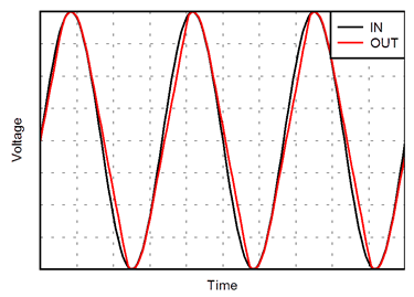
The full-power bandwidth of an amplifier describes the frequency at which the largest sinusoidal signal the amplifier can provide at the output before slew rate induced distortion becomes a dominant source of error. Figure 7-11 illustrates this concept.
 Figure 7-11 Slew Rate Induced Distortion
If the inputs of the amplifier are driven too far apart (such as when a multiplexer connected to the inverting input changes channels(, a slew boost circuit is enabled to help settling time, but can distort the signal. If low distortion is needed, avoid driving the inputs too far apart from each other. The OPAx828 have a full power bandwidth of 1.2 MHz with 10-VPEAK output voltage. Figure 7-12 illustrates the maximum output voltage as a function of frequency.