SBOS671D September 2018 – December 2022 OPA2828 , OPA828
PRODUCTION DATA
- 1 Features
- 2 Applications
- 3 Description
- 4 Revision History
- 5 Pin Configuration and Functions
- 6 Specifications
-
7 Detailed Description
- 7.1 Overview
- 7.2 Functional Block Diagram
- 7.3
Feature Description
- 7.3.1 Phase-Reversal Protection
- 7.3.2 Electrical Overstress
- 7.3.3 MUX Friendly Inputs
- 7.3.4 Overload Power Limiter
- 7.3.5 Noise Performance
- 7.3.6 Capacitive Load and Stability
- 7.3.7 Settling Time
- 7.3.8 Slew Rate
- 7.3.9 Full-Power Bandwidth
- 7.3.10 Small-Signal Response
- 7.3.11 Thermal Shutdown
- 7.3.12 Low Offset Voltage Drift
- 7.3.13 Overload Recovery
- 7.4 Device Functional Modes
- 8 Application and Implementation
- 9 Device and Documentation Support
- 10Mechanical, Packaging, and Orderable Information
Package Options
Mechanical Data (Package|Pins)
Thermal pad, mechanical data (Package|Pins)
- DGN|8
Orderable Information
7.3.7 Settling Time
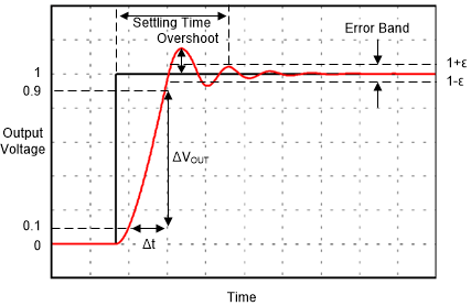
Settling time is a measure of an amplifier output to settle to within some percentage (error band) of the input amplitude and is used to describe an amplifier response to a step input. An amplifier settling time is comprised of both a large signal response and small signal response. The large signal response is characterized by the rise and fall times, whereas the small signal response is characterized by overshoot and ringing. Figure 7-10 illustrates the concepts and terminology associated with an amplifier settling time. Specifically, the settling time is defined as the time the output takes to settle to within a specified error band from the time the input signal was applied.
 Figure 7-10 Settling
Time
Figure 7-10 Settling
TimeThe OPAx828 minimize settling time for high-resolution systems in two ways. First, by incorporating an internal slew-boost circuit that minimizes rise and fall times, Second, by having wide bandwidth with excellent phase margin with low ringing, enabling small signal settling in minimal time. The OPAx828 are trimmed in laser production that minimizes part-to-part variation in the device slew rate, bandwidth, and phase margin, thus mainlining excellent unit-to-unit variations across all manufacturing lots.