SBOS671D September 2018 – December 2022 OPA2828 , OPA828
PRODUCTION DATA
- 1 Features
- 2 Applications
- 3 Description
- 4 Revision History
- 5 Pin Configuration and Functions
- 6 Specifications
-
7 Detailed Description
- 7.1 Overview
- 7.2 Functional Block Diagram
- 7.3
Feature Description
- 7.3.1 Phase-Reversal Protection
- 7.3.2 Electrical Overstress
- 7.3.3 MUX Friendly Inputs
- 7.3.4 Overload Power Limiter
- 7.3.5 Noise Performance
- 7.3.6 Capacitive Load and Stability
- 7.3.7 Settling Time
- 7.3.8 Slew Rate
- 7.3.9 Full-Power Bandwidth
- 7.3.10 Small-Signal Response
- 7.3.11 Thermal Shutdown
- 7.3.12 Low Offset Voltage Drift
- 7.3.13 Overload Recovery
- 7.4 Device Functional Modes
- 8 Application and Implementation
- 9 Device and Documentation Support
- 10Mechanical, Packaging, and Orderable Information
Package Options
Mechanical Data (Package|Pins)
Thermal pad, mechanical data (Package|Pins)
- DGN|8
Orderable Information
7.3.5 Noise Performance
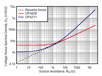
Figure 7-7 shows the total circuit noise for varying source impedances with the operational amplifier in a unity-gain configuration (with no feedback resistor network and therefore no additional noise contributions). The OPA828 and OPA211 are shown with total circuit noise calculated. The op amp contributes both a voltage noise component and a current noise component. The voltage noise is commonly modeled as a time-varying component of the offset voltage. The current noise is modeled as the time-varying component of the input bias current and reacts with the source resistance to create a voltage component of noise. Therefore, the lowest noise op amp for a given application depends on the source impedance. For low source impedance, current noise is negligible, and voltage noise generally dominates. The OPAx828 devices have both low voltage noise and extremely low current noise because of the FET input of the op amps. As a result, the current noise contribution of the OPAx828 is negligible for any practical source impedance, which makes the OPAx828 an excellent choice for applications with high source impedance.
Equation 2 provides a simple calculation for total noise, EO, of a unity gain buffer op amp circuit:
where
- eN = voltage noise
- iN = current noise
- RS = source impedance
- k = Boltzmann's constant = 1.38 × 10⁻²³ J/K
- T = temperature in kelvins (K)
 Figure 7-7 Noise
Performance of the OPA828 and OPA211 in Unity-Gain
Buffer Configuration