SBOS671D September 2018 – December 2022 OPA2828 , OPA828
PRODUCTION DATA
- 1 Features
- 2 Applications
- 3 Description
- 4 Revision History
- 5 Pin Configuration and Functions
- 6 Specifications
-
7 Detailed Description
- 7.1 Overview
- 7.2 Functional Block Diagram
- 7.3
Feature Description
- 7.3.1 Phase-Reversal Protection
- 7.3.2 Electrical Overstress
- 7.3.3 MUX Friendly Inputs
- 7.3.4 Overload Power Limiter
- 7.3.5 Noise Performance
- 7.3.6 Capacitive Load and Stability
- 7.3.7 Settling Time
- 7.3.8 Slew Rate
- 7.3.9 Full-Power Bandwidth
- 7.3.10 Small-Signal Response
- 7.3.11 Thermal Shutdown
- 7.3.12 Low Offset Voltage Drift
- 7.3.13 Overload Recovery
- 7.4 Device Functional Modes
- 8 Application and Implementation
- 9 Device and Documentation Support
- 10Mechanical, Packaging, and Orderable Information
Package Options
Mechanical Data (Package|Pins)
Thermal pad, mechanical data (Package|Pins)
- DGN|8
Orderable Information
7.3.1 Phase-Reversal Protection
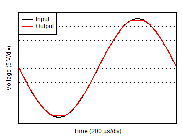
Many operational amplifiers exhibit a phase reversal when the input drives beyond the specified input common-mode range. This condition is most often encountered in noninverting circuits when the input drives beyond the specified common-mode voltage range, which can cause the output to reverse into the opposite rail. The OPAx828 have an internal phase-reversal protection circuitry. The input architecture of the OPAx828 prevents phase reversal with input common-mode voltages that exceed the specified maximum and minimum values. The OPAx828 output limits to the appropriate rail. Figure 7-1 shows this performance. When input voltages can exceed the minimum or maximum specified limits, make sure to limit the maximum input current through internal ESD protection diodes.
 Figure 7-1 No Phase
Reversal