SLAS666B January 2010 – October 2018 TLV320DAC3101
PRODUCTION DATA.
- 1Introduction
- 2Revision History
- 3Pin Configuration and Functions
-
4Specifications
- 4.1 Absolute Maximum Ratings
- 4.2 ESD Ratings
- 4.3 Recommended Operating Conditions
- 4.4 Thermal Information
- 4.5 Electrical Characteristics
- 4.6 Power Dissipation Ratings
- 4.7 I2S, LJF, and RJF Timing in Slave Mode
- 4.8 DSP Timing in Master Mode
- 4.9 DSP Timing in Slave Mode
- 4.10 I2C Interface Timing
- 4.11 Typical Characteristics
- 5Parameter Measurement Information
-
6Detailed Description
- 6.1 Overview
- 6.2 Functional Block Diagram
- 6.3
Feature Description
- 6.3.1 Power-Supply Sequence
- 6.3.2 Reset
- 6.3.3 Device Start-Up Lockout Times
- 6.3.4 PLL Start-Up
- 6.3.5 Power-Stage Reset
- 6.3.6 Software Power Down
- 6.3.7 Audio Analog I/O
- 6.3.8
Digital Processing Low-Power Modes
- 6.3.8.1 DAC Playback on Headphones, Stereo, 48 kHz, DVDD = 1.8 V, AVDD = 3.3 V, HPVDD = 3.3 V
- 6.3.8.2 DAC Playback on Headphones, Mono, 48 kHz, DVDD = 1.8 V, AVDD = 3.3 V, HPVDD = 3.3 V
- 6.3.8.3 DAC Playback on Headphones, Stereo, 8 kHz, DVDD = 1.8 V, AVDD = 3.3 V, HPVDD = 3.3 V
- 6.3.8.4 DAC Playback on Headphones, Mono, 8 kHz, DVDD = 1.8 V, AVDD = 3.3 V, HPVDD = 3.3 V
- 6.3.8.5 DAC Playback on Headphones, Stereo, 192 kHz, DVDD = 1.8 V, AVDD = 3.3 V, HPVDD = 3.3 V
- 6.3.8.6 DAC Playback on Line Out (10 k-Ω load), Stereo, 48 kHz, DVDD = 1.8 V, AVDD = 3 V, HPVDD = 3 V
- 6.3.9 Analog Signals
- 6.3.10
Audio DAC and Audio Analog Outputs
- 6.3.10.1
DAC
- 6.3.10.1.1 DAC Processing Blocks
- 6.3.10.1.2
DAC Processing Blocks — Details
- 6.3.10.1.2.1 Three Biquads, Filter A
- 6.3.10.1.2.2 Six Biquads, First-Order IIR, DRC, Filter A or B
- 6.3.10.1.2.3 Six Biquads, First-Order IIR, Filter A or B
- 6.3.10.1.2.4 IIR, Filter B or C
- 6.3.10.1.2.5 Four Biquads, DRC, Filter B
- 6.3.10.1.2.6 Four Biquads, Filter B
- 6.3.10.1.2.7 Four Biquads, First-Order IIR, DRC, Filter C
- 6.3.10.1.2.8 Four Biquads, First-Order IIR, Filter C
- 6.3.10.1.2.9 Two Biquads, 3D, Filter A
- 6.3.10.1.2.10 Five Biquads, DRC, 3D, Filter A
- 6.3.10.1.2.11 Five Biquads, DRC, 3D, Beep Generator, Filter A
- 6.3.10.1.3 DAC User-Programmable Filters
- 6.3.10.1.4 DAC Interpolation Filter Characteristics
- 6.3.10.2 DAC Digital-Volume Control
- 6.3.10.3 Volume Control Pin
- 6.3.10.4 Dynamic Range Compression
- 6.3.10.5 Headphone Detection
- 6.3.10.6 Interrupts
- 6.3.10.7 Key-Click Functionality With Digital Sine-Wave Generator (PRB_P25)
- 6.3.10.8 Programming DAC Digital Filter Coefficients
- 6.3.10.9 Updating DAC Digital Filter Coefficients During PLAY
- 6.3.10.10 Digital Mixing and Routing
- 6.3.10.11 Analog Audio Routing
- 6.3.10.12 Analog Outputs
- 6.3.10.13 Audio-Output Stage-Power Configurations
- 6.3.10.14 DAC Setup
- 6.3.10.15 Example Register Setup to Play Digital Data Through DAC and Headphone/Speaker Outputs
- 6.3.10.1
DAC
- 6.3.11 CLOCK Generation and PLL
- 6.3.12 Timer
- 6.3.13 Digital Audio and Control Interface
- 6.4
Register Map
- 6.4.1 Register Map
- 6.4.2
Registers
- 6.4.2.1
Control Registers, Page 0 (Default Page): Clock Multipliers, Dividers, Serial Interfaces, Flags, Interrupts, and GPIOs
- Table 6-31 Page 0 / Register 0 (0x00): Page Control Register
- Table 6-32 Page 0 / Register 1 (0x01): Software Reset
- Table 6-33 Page 0 / Register 2 (0x02): Reserved
- Table 6-34 Page 0 / Register 3 (0x03): OT FLAG
- Table 6-35 Page 0 / Register 4 (0x04): Clock-Gen Muxing
- Table 6-36 Page 0 / Register 5 (0x05): PLL P and R Values
- Table 6-37 Page 0 / Register 6 (0x06): PLL J-Value
- Table 6-38 Page 0 / Register 7 (0x07): PLL D-Value MSB
- Table 6-39 Page 0 / Register 8 (0x08): PLL D-Value LSB
- Table 6-40 Page 0 / Register 9 (0x09) and Page 0 / Register 10 (0x0A): Reserved
- Table 6-41 Page 0 / Register 11 (0x0B): DAC NDAC_VAL
- Table 6-42 Page 0 / Register 12 (0x0C): DAC MDAC_VAL
- Table 6-43 Page 0 / Register 13 (0x0D): DAC DOSR_VAL MSB
- Table 6-44 Page 0 / Register 14 (0x0E): DAC DOSR_VAL LSB
- Table 6-45 Page 0 / Register 15 (0x0F) through Page 0 / Register 24 (0x18): Reserved
- Table 6-46 Page 0 / Register 25 (0x19): CLKOUT MUX
- Table 6-47 Page 0 / Register 26 (0x1A): CLKOUT M_VAL
- Table 6-48 Page 0 / Register 27 (0x1B): Codec Interface Control 1
- Table 6-49 Page 0 / Register 28 (0x1C): Data-Slot Offset Programmability
- Table 6-50 Page 0 / Register 29 (0x1D): Codec Interface Control 2
- Table 6-51 Page 0 / Register 30 (0x1E): BCLK N_VAL
- Table 6-52 Page 0 / Register 31 (0x1F): Codec Secondary Interface Control 1
- Table 6-53 Page 0 / Register 32 (0x20): Codec Secondary Interface Control 2
- Table 6-54 Page 0 / Register 33 (0x21): Codec Secondary Interface Control 3
- Table 6-55 Page 0 / Register 34 (0x22): I2C Bus Condition
- Table 6-56 Page 0 / Register 35 (0x23) and Page 0 / Register 36 (0x24): Reserved
- Table 6-57 Page 0 / Register 37 (0x25): DAC Flag Register
- Table 6-58 Page 0 / Register 38 (0x26): DAC Flag Register
- Table 6-59 Page 0 / Register 39 (0x27): Overflow Flags
- Table 6-60 Page 0 / Register 40 (0x28) Through Page 0 / Register 43 (0x2B): Reserved
- Table 6-61 Page 0 / Register 44 (0x2C): DAC Interrupt Flags (Sticky Bits)
- Table 6-62 Page 0 / Register 45 (0x2D): Reserved
- Table 6-63 Page 0 / Register 46 (0x2E): Interrupt Flags—DAC
- Table 6-64 Page 0 / Register 47 (0x2F): Reserved
- Table 6-65 Page 0 / Register 48 (0x30): INT1 Control Register
- Table 6-66 Page 0 / Register 49 (0x31): INT2 Control Register
- Table 6-67 Page 0 / Register 50 (0x32): Reserved
- Table 6-68 Page 0 / Register 52 (0x34): Reserved
- Table 6-69 Page 0 / Register 53: Reserved
- Table 6-70 Page 0 / Register 54 (0x36): DIN (IN Pin) Control
- Table 6-71 Page 0 / Register 55 (0x37) through Page 0 / Register 59 (0x3B): Reserved
- Table 6-72 Page 0 / Register 60 (0x3C): DAC Processing Block Selection
- Table 6-73 Page 0 / Register 61 (0x3D)Through Page 0 / Register 62: Reserved
- Table 6-74 Page 0 / Register 63 (0x3F): DAC Data-Path Setup
- Table 6-75 Page 0 / Register 64 (0x40): DAC Volume Control
- Table 6-76 Page 0 / Register 65 (0x41): DAC Left Volume Control
- Table 6-77 Page 0 / Register 66 (0x42): DAC Right Volume Control
- Table 6-78 Page 0 / Register 67 (0x43): Headset Detection
- Table 6-79 Page 0 / Register 68 (0x44): DRC Control 1
- Table 6-80 Page 0 / Register 69 (0x45): DRC Control 2
- Table 6-81 Page 0 / Register 70 (0x46): DRC Control 3
- Table 6-82 Page 0 / Register 71 (0x47): Left Beep Generator
- Table 6-83 Page 0 / Register 72 (0x48): Right Beep Generator
- Table 6-84 Page 0 / Register 73 (0x49): Beep Length MSB
- Table 6-85 Page 0 / Register 74 (0x4A): Beep-Length Middle Bits
- Table 6-86 Page 0 / Register 75 (0x4B): Beep Length LSB
- Table 6-87 Page 0 / Register 76 (0x4C): Beep Sin(x) MSB
- Table 6-88 Page 0 / Register 77 (0x4D): Beep Sin(x) LSB
- Table 6-89 Page 0 / Register 78 (0x4E): Beep Cos(x) MSB
- Table 6-90 Page 0 / Register 79 (0x4F): Beep Cos(x) LSB
- Table 6-91 Page 0 / Register 80 (0x50) Through Page 0 / Register 115 (0x73): Reserved
- Table 6-92 Page 0 / Register 116 (0x74): VOL/MICDET-Pin SAR ADC — Volume Control
- Table 6-93 Page 0 / Register 117 (0x75): VOL/MICDET-Pin Gain
- Table 6-94 Page 0 / Register 118 (0x76) Through Page 0 / Register 127 (0x7F): Reserved
- 6.4.2.2
Control Registers, Page 1: DAC, Power-Controls, and MISC Logic-Related Programmability
- Table 6-95 Page 1 / Register 0 (0x00): Page Control Register
- Table 6-96 Page 1 / Register 1 (0x01) Through Page 1 / Register 29 (0x1D): Reserved
- Table 6-97 Page 1 / Register 30 (0x1E): Headphone and Speaker Amplifier Error Control
- Table 6-98 Page 1 / Register 31 (0x1F): Headphone Drivers
- Table 6-99 Page 1 / Register 32 (0x20): Class-D Speaker Amplifier
- Table 6-100 Page 1 / Register 33 (0x21): HP Output Drivers POP Removal Settings
- Table 6-101 Page 1 / Register 34 (0x22): Output Driver PGA Ramp-Down Period Control
- Table 6-102 Page 1 / Register 35 (0x23): DAC_L and DAC_R Output Mixer Routing
- Table 6-103 Page 1 / Register 36 (0x24): Left Analog Volume to HPL
- Table 6-104 Page 1 / Register 37 (0x25): Right Analog Volume to HPR
- Table 6-105 Page 1 / Register 38 (0x26): Left Analog Volume to SPL
- Table 6-106 Page 1 / Register 39 (0x27): Right Analog Volume to SPR
- Table 6-107 Page 1 / Register 40 (0x28): HPL Driver
- Table 6-108 Page 1 / Register 41 (0x29): HPR Driver
- Table 6-109 Page 1 / Register 42 (0x2A): SPL Driver
- Table 6-110 Page 1 / Register 43 (0x2B): SPR Driver
- Table 6-111 Page 1 / Register 44 (0x2C): HP Driver Control
- Table 6-112 Page 1 / Register 45 (0x2D): Reserved
- Table 6-113 Page 1 / Register 46 (0x2E): MICBIAS
- Table 6-114 Page 1 / Register 50 (0x32): Input CM Settings
- Table 6-115 Page 1 / Register 51 (0x33) Through Page 1 / Register 127 (0x7F): Reserved
- 6.4.2.3 Control Registers, Page 3: MCLK Divider for Programmable Delay Timer
- 6.4.2.4 Control Registers, Page 8: DAC Programmable Coefficients RAM Buffer A (1:63)
- 6.4.2.5 Control Registers, Page 9: DAC Programmable Coefficients RAM Buffer A (65:127)
- 6.4.2.6 Control Registers, Page 12: DAC Programmable Coefficients RAM Buffer B (1:63)
- 6.4.2.7 Control Registers, Page 13: DAC Programmable Coefficients RAM Buffer B (65:127)
- 6.4.2.1
Control Registers, Page 0 (Default Page): Clock Multipliers, Dividers, Serial Interfaces, Flags, Interrupts, and GPIOs
- 7Application and Implementation
- 8Power Supply Recommendations
- 9Layout
Package Options
Mechanical Data (Package|Pins)
- RHB|32
Thermal pad, mechanical data (Package|Pins)
- RHB|32
Orderable Information
6.3.11 CLOCK Generation and PLL
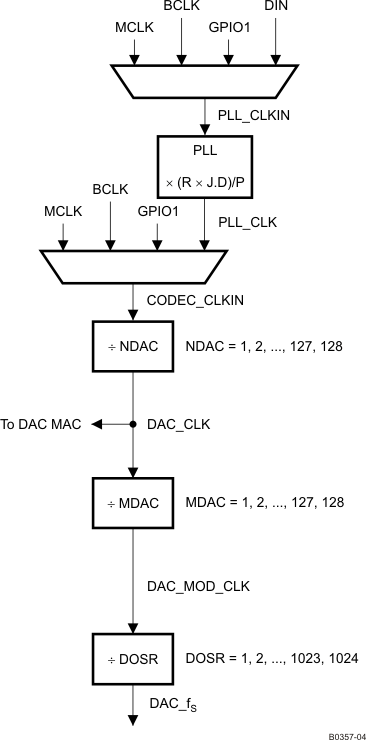
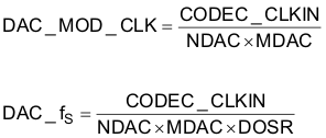
The device supports a wide range of options for generating clocks for the DAC section as well as interface and other control blocks as shown in Figure 6-19. The clocks for the DAC require a source reference clock. This clock is provided on a variety of device pins, such as the MCLK, BCLK, or GPIO1 pins. The source reference clock for the codec is chosen by programming the CODEC_CLKIN value on page 0 / register 4, bits D1–D0. The CODEC_CLKIN is then routed through highly-flexible clock dividers shown in Figure 6-19 to generate the various clocks required for the DAC. In the event that the desired audio clocks cannot be generated from the reference clocks on MCLK, BCLK, or GPIO1, the device also provides the option of using the on-chip PLL which supports a wide range of fractional multiplication values to generate the required clocks. Starting from CODEC_CLKIN, the device provides several programmable clock dividers to help achieve a variety of sampling rates for the DAC.
 Figure 6-19 Clock Distribution Tree
Table 6-26 CODEC CLKIN Clock Dividers
| DIVIDER | BITS |
|---|---|
| NDAC | Page 0 / register 11, bits D6–D0 |
| MDAC | Page 0 / register 12, bits D6–D0 |
| DOSR | Page 0 / register 13, bits D1–D0 and page 0 / register 14, bits D7–D0 |
The DAC modulator is clocked by DAC_MOD_CLK. For proper power-up operation of the DAC channel, DAC_MOD_CLK must be enabled by configuring the NDAC and MDAC clock dividers (page 0 / register 11, bit D7 = 1 and page 0 / register 12, bit D7 = 1). When the DAC channel is powered down, the device internally initiates a power-down sequence for proper shutdown. During this shutdown sequence, the NDAC and MDAC dividers must not be powered down, or else a proper low-power shutdown may not take place. The user can read back the power-status flag at page 0 / register 37, bit D7 and page 0 / register 37, bit D3. When both of the flags indicate power-down, the MDAC divider may be powered down, followed by the NDAC divider.
In general, for proper operation, all the root clock dividers must power down only after the child clock dividers have powered down.
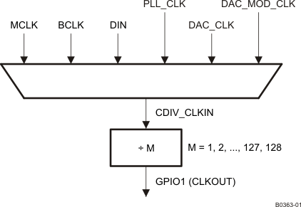
The device also has options for routing some of the internal clocks to the GPIO1 pin to be used as general-purpose clocks in the system. The feature is shown in Figure 6-21.
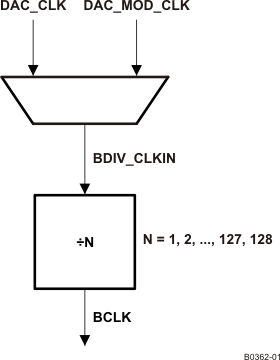
 Figure 6-20 BCLK Output Options
 In the mode when the device is configured to drive the BCLK pin (page 0 / register 27, bit D3 = 1), the device is driven as the divided value of BDIV_CLKIN. The division value is programmed in page 0 / register 30, bits D6–D0 from 1 to 128. The BDIV_CLKIN is configurable to be one of DAC_CLK (DAC processing clock) or DAC_MOD_CLK by configuring the BDIV_CLKIN multiplexer in page 0 / register 29, bits D1–D0. Additionally, a general-purpose clock can be driven out on GPIO1.
This clock can be a divided-down version of CDIV_CLKIN. The value of this clock divider can be programmed from 1 to 128 by writing to page 0 / register 26, bits D6–D0. CDIV_CLKIN can also be programmed as one of the clocks among the list shown in Figure 6-21. This is controlled by programming the multiplexer in page 0 / register 25, bits D2–D0.
 Figure 6-21 General-Purpose Clock Output Options
 Table 6-27 Maximum Clock Frequencies
| CLOCK | DVDD ≥ 1.65 V |
|---|---|
| CODEC_CLKIN | ≤ 110 MHz |
| DAC_CLK (DAC processing clock) | ≤ 49.152 MHz |
| DAC_MOD_CLK | ≤ 49.152 MHz with DRC disabled
≤ 48 MHz with DRC enabled |
| DAC_MOD_CLK | 6.758 MHz |
| DAC_fS | 0.192 MHz |
| BDIV_CLKIN | 55 MHz |
| CDIV_CLKIN | 100 MHz when M is odd
110 MHz when M is even |