JAJSKL8E june 2006 – october 2020 SN65LVDS302
PRODUCTION DATA
- 1
- 1 特長
- 2 アプリケーション
- 3 概要
- 4 Revision History
- 5 Pin Configuration and Functions
-
6 Specifications
- 6.1 Absolute Maximum Ratings
- 6.2 ESD Ratings
- 6.3 Recommended Operating Conditions
- 6.4 Thermal Information
- 6.5 Electrical Characteristics
- 6.6 Input Electrical Characteristics
- 6.7 Output Electrical Characteristics
- 6.8 Timing Requirements
- 6.9 Switching Characteristics
- 6.10 Device Power Dissipation
- Typical Characteristics
- 7 Parameter Measurement Information
- 8 Detailed Description
-
9 Application and Implementation
- 9.1
Application Information
- 9.1.1 Application Information
- 9.1.2 Preventing Increased Leakage Currents in Control Inputs
- 9.1.3 Calculation Example: HVGA Display
- 9.1.4 How to Determine Interconnect Skew and Jitter Budget
- 9.1.5 F/S Pin Setting and Connecting the SN65LVDS302 to an LCD Driver
- 9.1.6 How to Determine the LCD Driver Timing Margin
- 9.1.7 Typical Application Frequencies
- 9.2 Typical Applications
- 9.1
Application Information
- 10Power Supply Recommendations
- 11Layout
- 12Device and Documentation Support
- 13Mechanical, Packaging, and Orderable Information
8.3.2 Parity Error Detection and Handling
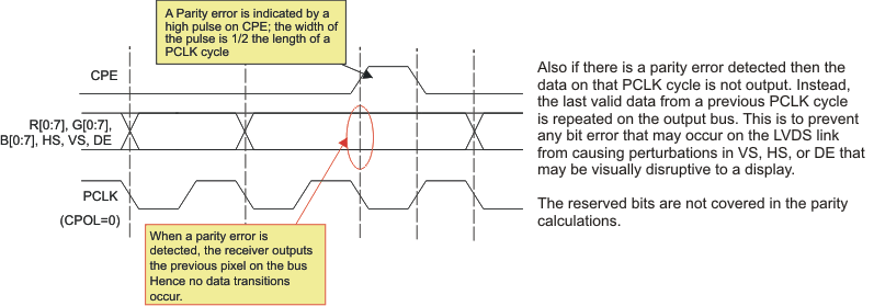
The SN65LVDS302 receiver performs error checking on the basis of a parity bit that is transmitted across the subLVDS interface from the transmitting device. Once the SN65LVDS302 detects the presence of the clock and the PLL has locked onto PCLK, then the parity is checked. Parity-error detection ensures detection of all single bit errors in one pixel and 50% of all multi-bit errors.
The parity bit covers the 27 bit data payload consisting of 24 bits of pixel data plus VS, HS, and DE. Odd Parity bit signalling is used. The parity error is output on the CPE pin. If the sum of the 27 data bits and the parity bit result in an odd number, the receive data are assumed to be valid. The CPE output is held low. If the sum equals an even number, parity error is declared. The CPE output indicates high for half a PCLK period. The CPE output is set with the data bit transition and cleared after 1/2 the data bit time. This allows counting every detected parity error with a simple counter connected to CPE.
 Figure 8-3 Parity Error Detection and Handling