JAJSKL8E june 2006 – october 2020 SN65LVDS302
PRODUCTION DATA
- 1
- 1 特長
- 2 アプリケーション
- 3 概要
- 4 Revision History
- 5 Pin Configuration and Functions
-
6 Specifications
- 6.1 Absolute Maximum Ratings
- 6.2 ESD Ratings
- 6.3 Recommended Operating Conditions
- 6.4 Thermal Information
- 6.5 Electrical Characteristics
- 6.6 Input Electrical Characteristics
- 6.7 Output Electrical Characteristics
- 6.8 Timing Requirements
- 6.9 Switching Characteristics
- 6.10 Device Power Dissipation
- Typical Characteristics
- 7 Parameter Measurement Information
- 8 Detailed Description
-
9 Application and Implementation
- 9.1
Application Information
- 9.1.1 Application Information
- 9.1.2 Preventing Increased Leakage Currents in Control Inputs
- 9.1.3 Calculation Example: HVGA Display
- 9.1.4 How to Determine Interconnect Skew and Jitter Budget
- 9.1.5 F/S Pin Setting and Connecting the SN65LVDS302 to an LCD Driver
- 9.1.6 How to Determine the LCD Driver Timing Margin
- 9.1.7 Typical Application Frequencies
- 9.2 Typical Applications
- 9.1
Application Information
- 10Power Supply Recommendations
- 11Layout
- 12Device and Documentation Support
- 13Mechanical, Packaging, and Orderable Information
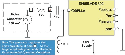 Figure 7-1 Power
Supply Noise Test Set-Up
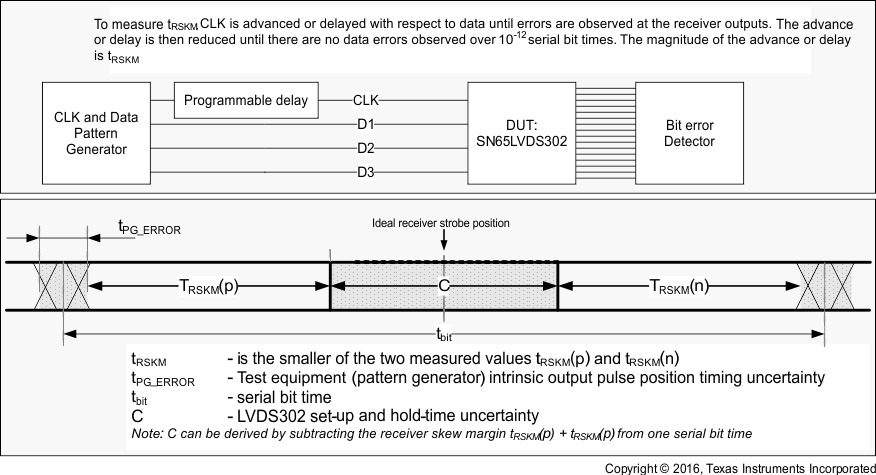 Figure 7-2 Jitter
Budget
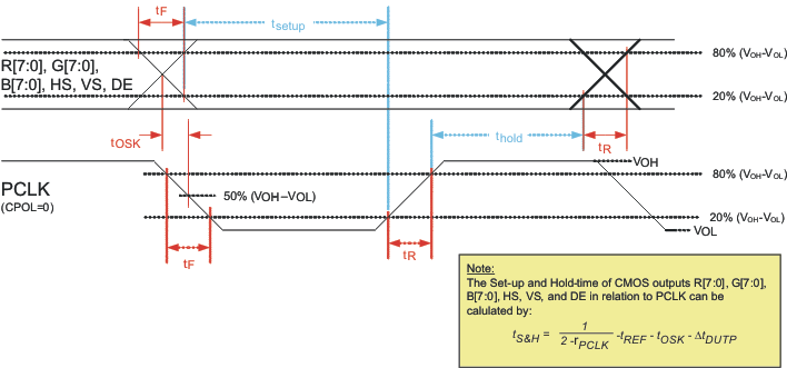 Figure 7-3 Output
Rise and Fall, Setup and Hold Time
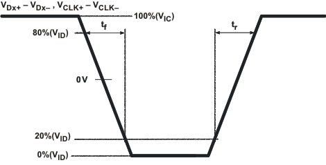 Figure 7-4 SubLVDS
Differential Input Rise and Fall Time Defintion
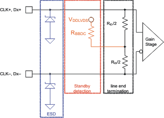 Figure 7-5 Equivalent Input Circuit Design
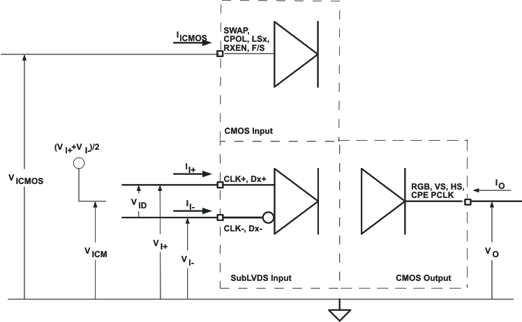 Figure 7-6 I/O
Voltage and Current Definition
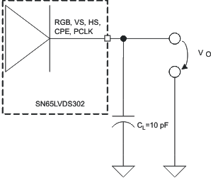 Figure 7-7 CMOS
Output Test Circuit, Signal and Timing Definition
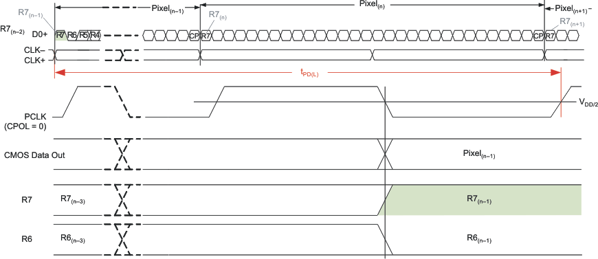 Figure 7-8 Propagation Delay Input to Output (LS0 = LS1 = 0)
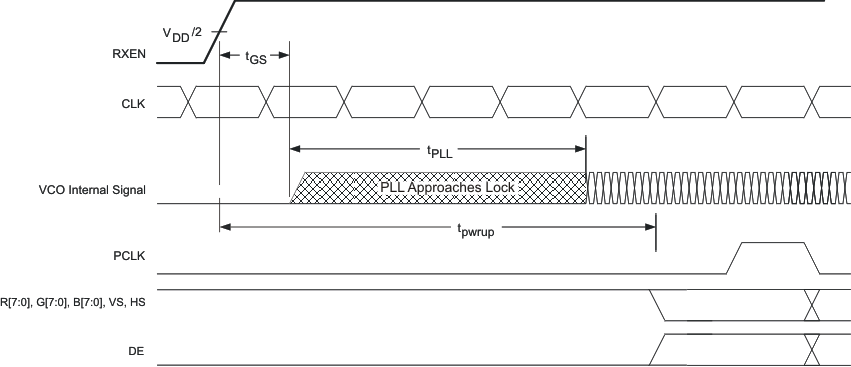 Figure 7-9 Receiver
Phase Lock Loop Set Time and Receiver Enable Time
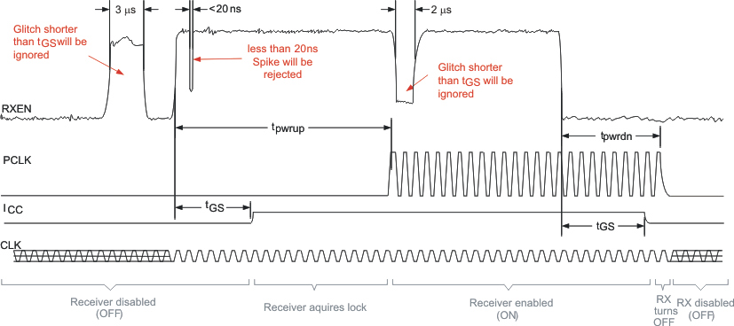 Figure 7-10 Receiver
Enable and Disable Glitch Suppression Time
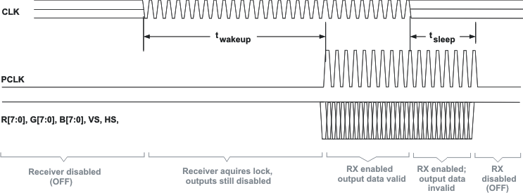 Figure 7-11 Standby
Detection