JAJSCG5C July 2016 – June 2018 TPS546C23
PRODUCTION DATA.
- 1 特長
- 2 アプリケーション
- 3 概要
- 4 改訂履歴
- 5 Pin Configuration and Functions
- 6 Specifications
-
7 Detailed Description
- 7.1 Overview
- 7.2 Functional Block Diagram
- 7.3
Feature Description
- 7.3.1 2-Phase Application
- 7.3.2 Linear Regulators BP3 and BP6
- 7.3.3 Input Undervoltage Lockout (UVLO)
- 7.3.4 Turnon and Turnoff Delay and Sequencing
- 7.3.5 Voltage Reference
- 7.3.6 Differential Remote Sense and Compensation
- 7.3.7 Set Output Voltage and Adaptive Voltage Scaling (AVS)
- 7.3.8 Reset VOUT
- 7.3.9 Switching Frequency and Synchronization
- 7.3.10 Current Sharing
- 7.3.11 Soft-Start Time and TON_RISE Command
- 7.3.12 Prebiased Output Start-Up
- 7.3.13 Soft-Stop time and TOFF_FALL Command
- 7.3.14 Output Current Telemetry and Low-Side MOSFET Overcurrent Protection
- 7.3.15 High-Side MOSFET Short-Circuit Protection
- 7.3.16 Die Temperature Telemetry and Overtemperature Protection
- 7.3.17 Output Voltage Telemetry and Over-/Under-voltage Protection
- 7.3.18 TON_MAX Fault
- 7.3.19 Power Good (PGOOD) Indicator
- 7.3.20 Fault Protection Responses
- 7.3.21 Switching Node
- 7.3.22 PMBus General Description
- 7.3.23 PMBus Address
- 7.3.24 PMBus Connections
- 7.3.25 Auto ARA (Alert Response Address) Response
- 7.4 Device Functional Modes
- 7.5 Programming
- 7.6
Register Maps
- 7.6.1 OPERATION (01h)
- 7.6.2 ON_OFF_CONFIG (02h)
- 7.6.3 CLEAR_FAULTS (03h)
- 7.6.4 WRITE_PROTECT (10h)
- 7.6.5 STORE_DEFAULT_ALL (11h)
- 7.6.6 RESTORE_DEFAULT_ALL (12h)
- 7.6.7 STORE_USER_ALL (11h)
- 7.6.8 RESTORE_USER_ALL (12h)
- 7.6.9 CAPABILITY (19h)
- 7.6.10 SMBALERT_MASK (1Bh)
- 7.6.11 VOUT_MODE (20h)
- 7.6.12 VOUT_COMMAND (21h)
- 7.6.13 VOUT_MAX (24h)
- 7.6.14 VOUT_TRANSITION_RATE (27h)
- 7.6.15 VOUT_SCALE_LOOP (29h)
- 7.6.16 VOUT_MIN (2Bh)
- 7.6.17 VIN_ON (35h)
- 7.6.18 VIN_OFF (36h)
- 7.6.19 IOUT_CAL_OFFSET (39h)
- 7.6.20 VOUT_OV_FAULT_RESPONSE (41h)
- 7.6.21 VOUT_UV_FAULT_RESPONSE (45h)
- 7.6.22 IOUT_OC_FAULT_LIMIT (46h)
- 7.6.23 IOUT_OC_FAULT_RESPONSE (47h)
- 7.6.24 IOUT_OC_WARN_LIMIT (4Ah)
- 7.6.25 OT_FAULT_LIMIT (4Fh)
- 7.6.26 OT_FAULT_RESPONSE (50h)
- 7.6.27 OT_WARN_LIMIT (51h)
- 7.6.28 TON_DELAY (60h)
- 7.6.29 TON_RISE (61h)
- 7.6.30 TON_MAX_FAULT_LIMIT (62h)
- 7.6.31 TON_MAX_FAULT_RESPONSE (63h)
- 7.6.32 TOFF_DELAY (64h)
- 7.6.33 TOFF_FALL (65h)
- 7.6.34 STATUS_BYTE (78h)
- 7.6.35 STATUS_WORD (79h)
- 7.6.36 STATUS_VOUT (7Ah)
- 7.6.37 STATUS_IOUT (7Bh)
- 7.6.38 STATUS_INPUT (7Ch)
- 7.6.39 STATUS_TEMPERATURE (7Dh)
- 7.6.40 STATUS_CML (7Eh)
- 7.6.41 STATUS_MFR_SPECIFIC (80h)
- 7.6.42 READ_VOUT (8Bh)
- 7.6.43 READ_IOUT (8Ch)
- 7.6.44 READ_TEMPERATURE_1 (8Dh)
- 7.6.45 PMBUS_REVISION (98h)
- 7.6.46 IC_DEVICE_ID (ADh)
- 7.6.47 IC_DEVICE_REV (AEh)
- 7.6.48 MFR_SPECIFIC_00 (D0h)
- 7.6.49 VREF_TRIM (MFR_SPECIFIC_04) (D4h)
- 7.6.50 STEP_VREF_MARGIN_HIGH (MFR_SPECIFIC_05) (D5h)
- 7.6.51 STEP_VREF_MARGIN_LOW (MFR_SPECIFIC_06) (D6h)
- 7.6.52 PCT_OV_UV_WRN_FLT_LIMITS (MFR_SPECIFIC_07) (D7h)
- 7.6.53 OPTIONS (MFR_SPECIFIC_21) (E5h)
- 7.6.54 MISC_CONFIG_OPTIONS (MFR_SPECIFIC_32) (F0h)
-
8 Application and Implementation
- 8.1 Application Information
- 8.2
Typical Application
- 8.2.1
4.5-V to 18-V Input, 1-V Typical Output, 35-A Converter
- 8.2.1.1 Design Requirements
- 8.2.1.2
Detailed Design Procedure
- 8.2.1.2.1 Custom Design With WEBENCH® Tools
- 8.2.1.2.2 Switching Frequency Selection
- 8.2.1.2.3 Inductor Selection
- 8.2.1.2.4 Output Capacitor Selection
- 8.2.1.2.5 Output Voltage Deviation During Load Transient
- 8.2.1.2.6 Output Voltage Ripple
- 8.2.1.2.7 Input Capacitor Selection
- 8.2.1.2.8 AVIN, BP6, BP3 Bypass Capacitor
- 8.2.1.2.9 Bootstrap Capacitor Selection
- 8.2.1.2.10 R-C Snubber
- 8.2.1.2.11 Output Voltage Setting and Frequency Compensation Selection
- 8.2.1.2.12 Key PMBus Parameter Selection
- 8.2.1.2.13 Enable, UVLO
- 8.2.1.2.14 Soft-Start Time
- 8.2.1.2.15 Overcurrent Threshold and Response
- 8.2.1.3 Application Curves
- 8.2.1
4.5-V to 18-V Input, 1-V Typical Output, 35-A Converter
- 9 Power Supply Recommendations
- 10Layout
- 11デバイスおよびドキュメントのサポート
- 12メカニカル、パッケージ、および注文情報
パッケージ・オプション
メカニカル・データ(パッケージ|ピン)
- RVF|40
サーマルパッド・メカニカル・データ
- RVF|40
発注情報
7.3.6 Differential Remote Sense and Compensation
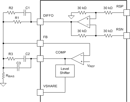
The devices implement a differential remote-sense amplifier to provide excellent load regulation by cancelling IR-drop in high-current applications. The RSP and RSN pins should be kelvin-connected to the output capacitor bank directly at the load, and routed back to the device as a tightly coupled differential pair. Ensure that these traces are isolated from fast switching signals and high current paths on the final PCB layout, as these can add differential-mode noise. Optionally, use a small coupling capacitor (1-nF typical) between the RSP and RSN pins to improve noise immunity. The output of the differential remote sense amplifier (DIFFO) is used for output voltage setting and error amplifier frequency compensation local to the device as shown in Figure 25.
The devices use voltage mode control with input feedforward. Frequency compensation can be accomplished using standard Type III techniques as shown in Figure 25.
In 2-phase configuration, the FB pin of the loop slave device should be tied to BP3 and the typical application circuit is shown in Figure 23. The loop master passes the internal COMP voltage through VSHARE pin to the loop slave device. For more information, see the Current Sharing section.
Additionally, the voltage at the DIFFO pin is digitized, averaged to reduce measurement noise and continually stored in the READ_VOUT command, enabling output voltage telemetry.
 Figure 25. Output Voltage Setting