JAJU510H March 2018 – December 2022
- 概要
- リソース
- 特長
- アプリケーション
- 5
- 1System Description
- 2System Overview
-
3Hardware, Software, Testing Requirements, and Test Results
- 3.1 Required Hardware and Software
- 3.2 Testing and Results
- 4Design Files
- 5Trademarks
- 6About the Authors
- 7Revision History
3.2.3.2 Lab 6
In this build level the current loop for the PFC is checked. Lab 6 is primarily meant for tuning the current loop and optimizing its performance. It is always safe to start Lab 6 at low voltage and low power as starting at higher power without a supervisory voltage loop can boost the voltage due to overcurrent events and can blow away the switches. Hence, it is very important to carefully set the TINV_idRef_pu variable so as to avoid overcurrent trips and high voltages at the DC terminals. Also the TINV_idRef_pu is defined with a negative sign for PFC mode of operation and with a positive sign for inverter mode of operation.
Figure 3-21 describes the software flow for running Lab 6.
Set the project to Lab 6 by changing the Lab Number in the <settings.h> file, (this will be changed by powerSUITE GUI when using powerSUITE project)
In the user settings.h file some additional options are available, but the following are used for the tests documented in this user guide.
#if TINV_LAB == 6
#define TINV_TEST_SETUP TINV_TEST_SETUP_RES_LOAD
#define TINV_PROTECTION TINV_PROTECTION_ENABLED
#define TINV_SFRA_TYPE TINV_SFRA_CURRENT
#define TINV_SFRA_AMPLITUDE (float32_t)TINV_SFRA_INJECTION_AMPLITUDE_LEVEL2
#define TINV_POWERFLOW_MODE TINV_RECTIFIERER_MODE
#define TINV_DC_CHECK 0
#define TINV_SPLL_TYPE TINV_SPLL_SRF
#endif
In this check the SW is run on the hardware, or the HIL platform, or both.
Refer to the hardware test set up section for actual details of the equipment used for configuring the test. Do not supply any HV power yet to the board.
- First launch the main.cfg and select Lab 6 in the project options. The compensator style (PI compensator) and the tuning loop (current loop) will be automatically populated. Now click run compensation designer icon and compensation designer tool will launch, with the model of the current loop plant with parameters specified on the powerSUITE page.
- The current compensator coefficients used for running the control loop are shown
in the following code. The user can modify these coefficients to meet the
necessary loop bandwidth and phase margin. The ideal coefficients with resistive
load are slightly different than the one used for grid connection because the
grid impedance is very low. The compensator design transfer function and
response are shown in Figure 3-22.
#define TINV_GI_PI_KP ((float32_t)0.3)) #define TINV_GI_PI_KI ((float32_t)0.0120860479))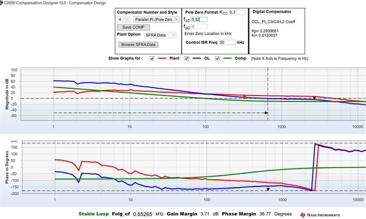 Figure 3-22 Compensator Design GUI
- Current Loop PI Coefficients
 - Once satisfied with the proportional and integral gain values, click on Save COMP. This will save the compensator values into the project. Close the Compensation Designer, and return to the powerSUITE page.
- Turn on the auxiliary power supply and set it to 15 V. Build and load the code, use the lab6.js file to populate the watch variables in the CCS window.
- Set the load resistance to a high value 3.18 kΩ.
- Set the AC input voltage to 30 VRMS with appropriate current limit.
- After turning on the AC power supply, immediately turn on the relay by writing a 1 to TINV_allRelaySet. Ensure that the relay is turned on immediately (within 3-4 seconds) after turning on the ac supply.
- Set TINV_idRef_pu to –0.013 pu
- To start the PFC mode, enter "1" on TINV_startPowerStage variable, the current should now be drawn from the grid as a sinusoidal signal (with some harmonics as it is at low power) and boost action seen on the vBus. The output voltage will boost from 75 V to around 180 V as shown in Figure 3-23.
- The current will become sinusoidal as the load is increased. This verifies start up of PFC at 30 VRMS.
- The Figure 3-23
shows PFC closed current loop start up at 30 VRMS. Scope
signals: Channel 1 - AC voltage (blue), Channel 2- DC voltage (light
green), Channel 3 - AC current (dark green).
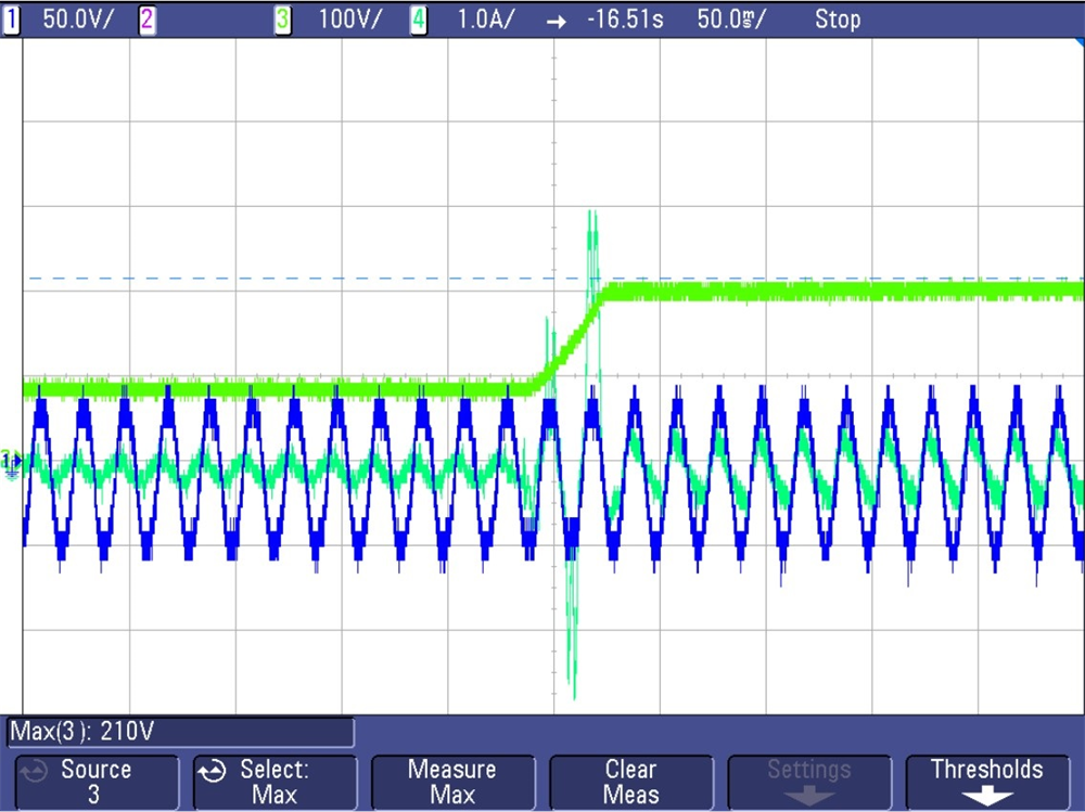 Figure 3-23 PFC Current Loop Start-up at 30 VRMS
 - Now repeat the previous steps to verify start up at 220 VRMS.
At 220 VRMS, with the TINV_idRef_pu set to –0.013 pu, the bus voltage jumps from 550 V to 640 V at 155 W power as Figure 3-24 shows.
- Figure 3-24 shows
PFC closed current loop start up at 220 VRMS. Scope signals:
Channel 1 - AC voltage (blue), Channel 2 - DC voltage (light green), Channel 3 -
AC current (dark green)
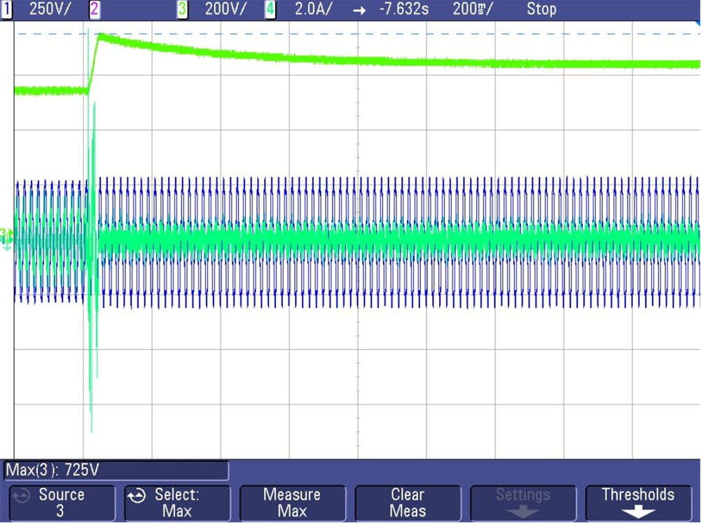 Figure 3-24 PFC Current Loop Start-up at 220 VRMS
 - As Figure 3-24 shows, running this lab at higher input voltage without a supervisory voltage loop results in big overvoltage across the DC terminals. Hence it is always advisable to start this lab at low voltage and low power as previously described for safety reasons and then slowly ramp to the desired voltage for closed current loop tuning. Starting at 230-VRMS AC input voltage and boosting DC voltage to 800 V directly is shown in Lab 7.
- In case any overcurrent trip is observed which causes the PWMs to switch off, please refer the notes in Lab 5 to debug this condition.
- A soft start scheme is implemented at the start-up to ensure overcurrents are
reduced at start-up. For this the duty is restricted to the PWM module by
adjusting the dead band set Figure 3-25 shows
the PWM configuration for this setup where the dead band is set to large value
and slowly reduced to the nominal value to limit the current spikes.
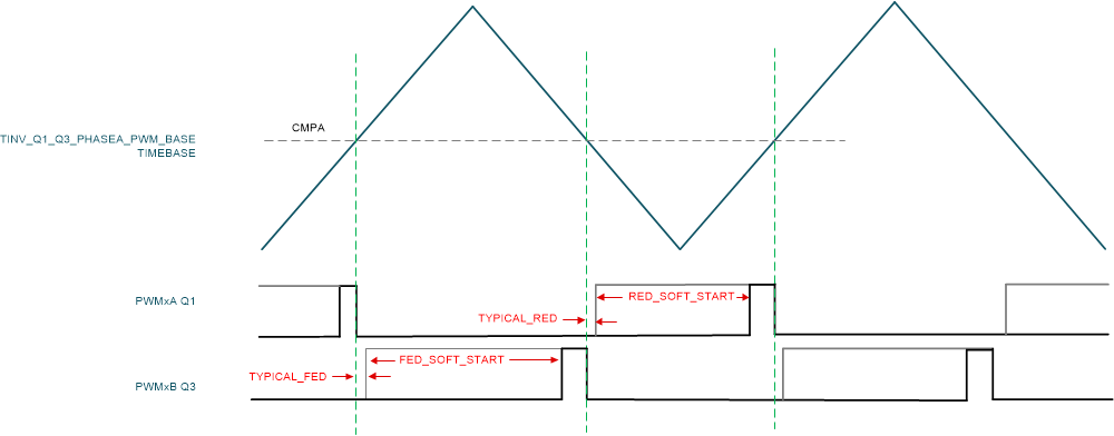 Figure 3-25 Dead Band Soft Start PWM Configuration
- Figure 3-26 shows
the effect of the start-up scheme without dead band implemented at start-up.
Without soft start, a huge current spike appears which causes over current trip
and the DC bus voltage also collapses. Figure 3-26 shows
overcurrent without soft-start implementation. Channel 1 - AC voltage (blue),
Channel 2 - AC current (light green), Channel 3 - DC voltage (dark green)
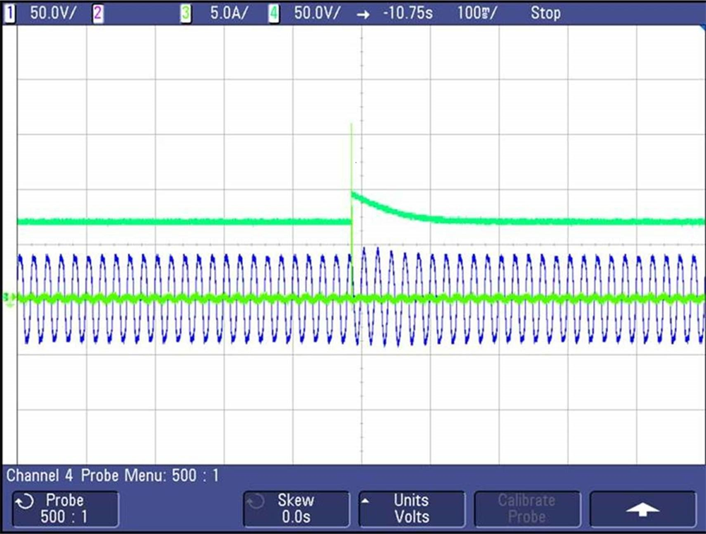 Figure 3-26 Without Soft Start
Figure 3-27 shows reduced current spike with soft-start implementation. Channel 1 - AC voltage (blue), Channel 2 - AC current (light green), Channel 3 - DC voltage (dark green).
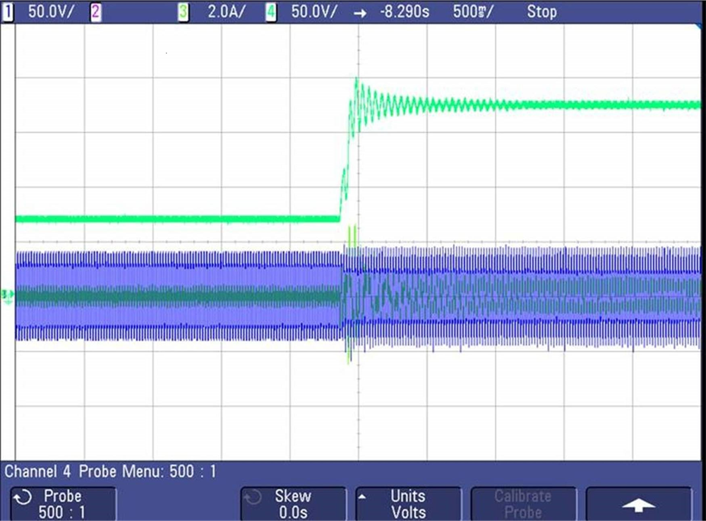 Figure 3-27 Soft Start With Adaptive Dead Band
- SFRA is integrated in the software of this lab to verify the designed compensator provides enough gain and phase margin by measuring on hardware. To run the SFRA keep the project running, and from the cfg page, click on the SFRA icon. SFRA GUI will pop up.
- Select the options for the device on the SFRA GUI. For example, for F28377D select floating point. Click on Setup Connection. On the pop-up window uncheck the boot on connect option, and select an appropriate COM port. Click OK. Return to the SFRA GUI, and click Connect.
- The SFRA GUI will connect to the device. A SFRA sweep can now be started by
clicking Start Sweep. The complete SFRA sweep will take a few minutes to finish.
Activity can be monitored by seeing the progress bar on the SFRA GUI and also
checking the flashing of blue LED on the back on the control card that indicates
UART activity. Once complete, a graph with the open loop plot will appear, as in
Figure 3-28
and Figure 3-29
which corresponds to plant and loop response measured by SFRA GUI respectively.
This verifies that the designed compensator is indeed stable
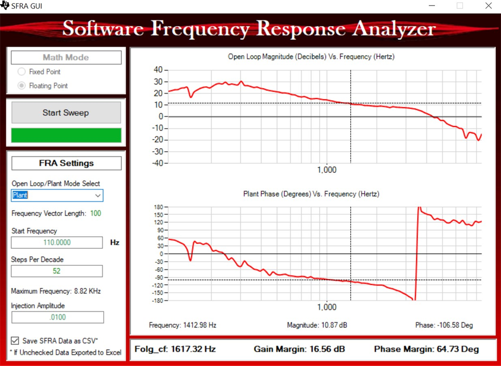 Figure 3-28 PFC SFRA Plant Response for Current Loop
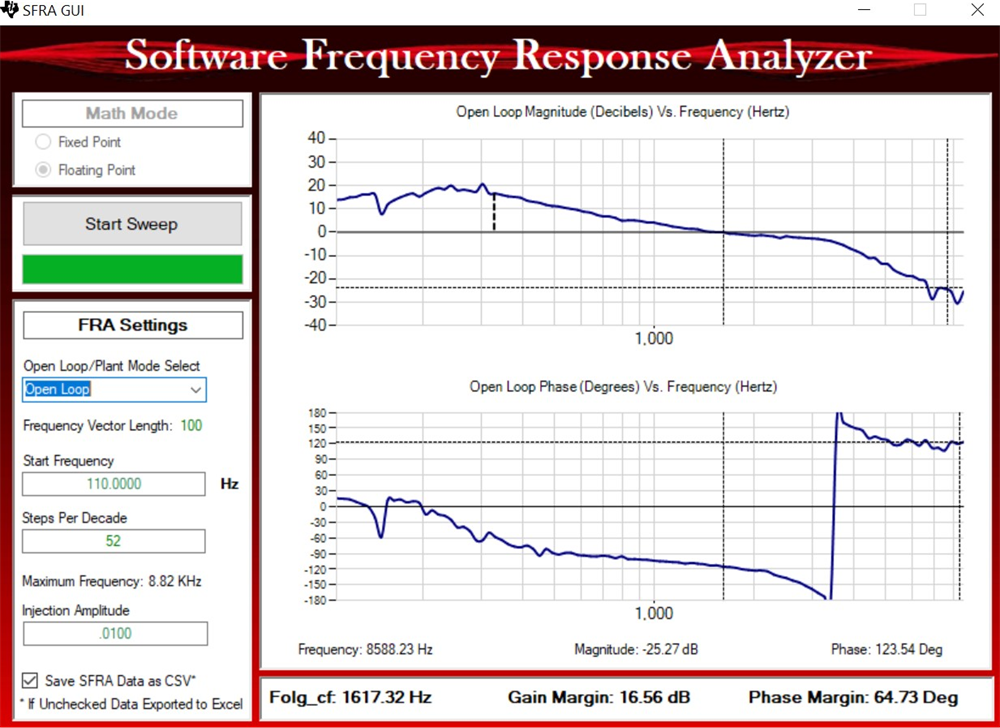 Figure 3-29 PFC SFRA Loop Response for Current Loop
 - The frequency response data is also saved in the project folder under an SFRA data folder and is time stamped with the time of the SFRA run.
- This completes verification of Lab 6.