JAJU510H March   2018  – December 2022


  1.   概要
  2.   リソース
  3.   特長
  4.   アプリケーション
  5.   5
  6. 1System Description
    1. 1.1 Key System Specifications
  7. 2System Overview
    1. 2.1 Block Diagram
    2. 2.2 Highlighted Products
      1. 2.2.1  UCC21710
      2. 2.2.2  UCC5320
      3. 2.2.3  TMS320F28379D
      4. 2.2.4  AMC1305M05
      5. 2.2.5  OPA4340
      6. 2.2.6  LM76003
      7. 2.2.7  PTH08080W
      8. 2.2.8  TLV1117
      9. 2.2.9  OPA350
      10. 2.2.10 UCC14240
    3. 2.3 System Design Theory
      1. 2.3.1 Three-Phase T-Type Inverter
        1. 2.3.1.1 Architecture Overview
        2. 2.3.1.2 LCL Filter Design
        3. 2.3.1.3 Inductor Design
        4. 2.3.1.4 SiC MOSFETs Selection
        5. 2.3.1.5 Loss Estimations
        6. 2.3.1.6 Thermal Considerations
      2. 2.3.2 Voltage Sensing
      3. 2.3.3 Current Sensing
      4. 2.3.4 System Power Supplies
        1. 2.3.4.1 Main Input Power Conditioning
        2. 2.3.4.2 Isolated Bias Supplies
      5. 2.3.5 Gate Drivers
        1. 2.3.5.1 1200-V SiC MOSFETs
        2. 2.3.5.2 650-V SiC MOSFETs
        3. 2.3.5.3 Gate Driver Bias Supply
      6. 2.3.6 Control Design
        1. 2.3.6.1 Current Loop Design
        2. 2.3.6.2 PFC DC Bus Voltage Regulation Loop Design
  8. 3Hardware, Software, Testing Requirements, and Test Results
    1. 3.1 Required Hardware and Software
      1. 3.1.1 Hardware
        1. 3.1.1.1 Test Hardware Required
        2. 3.1.1.2 Microcontroller Resources Used on the Design
        3. 3.1.1.3 F28377D, F28379D Control-Card Settings
      2. 3.1.2 Software
        1. 3.1.2.1 Getting Started With Firmware
          1. 3.1.2.1.1 Opening the CCS project
          2. 3.1.2.1.2 Digital Power SDK Software Architecture
          3. 3.1.2.1.3 Interrupts and Lab Structure
          4. 3.1.2.1.4 Building, Loading and Debugging the Firmware
        2. 3.1.2.2 Protection Scheme
        3. 3.1.2.3 PWM Switching Scheme
        4. 3.1.2.4 ADC Loading
    2. 3.2 Testing and Results
      1. 3.2.1 Lab 1
      2. 3.2.2 Testing Inverter Operation
        1. 3.2.2.1 Lab 2
        2. 3.2.2.2 Lab 3
        3. 3.2.2.3 Lab 4
      3. 3.2.3 Testing PFC Operation
        1. 3.2.3.1 Lab 5
        2. 3.2.3.2 Lab 6
        3. 3.2.3.3 Lab 7
      4. 3.2.4 Test Setup for Efficiency
      5. 3.2.5 Test Results
        1. 3.2.5.1 PFC Mode - 230 VRMS, 400 V L-L
          1. 3.2.5.1.1 PFC Start-up – 230 VRMS, 400 L-L AC Voltage
          2. 3.2.5.1.2 Steady State Results at 230 VRMS, 400 V L-L - PFC Mode
          3. 3.2.5.1.3 Efficiency and THD Results at 220 VRMS, 50 Hz – PFC Mode
          4. 3.2.5.1.4 Transient Test With Step Load Change
        2. 3.2.5.2 PFC Mode - 120 VRMS, 208 V L-L
          1. 3.2.5.2.1 Steady State Results at 120 VRMS, 208 V-L-L - PFC Mode
          2. 3.2.5.2.2 Efficiency and THD Results at 120 VRMS - PFC Mode
        3. 3.2.5.3 Inverter Mode
          1. 3.2.5.3.1 Inverter Closed Loop Results
          2. 3.2.5.3.2 Efficiency and THD Results - Inverter Mode
          3. 3.2.5.3.3 Inverter - Transient Test
      6. 3.2.6 Open Loop Inverter Test Results
  9. 4Design Files
    1. 4.1 Schematics
    2. 4.2 Bill of Materials
    3. 4.3 PCB Layout Recommendations
      1. 4.3.1 Layout Prints
    4. 4.4 Altium Project
    5. 4.5 Gerber Files
    6. 4.6 Assembly Drawings
  10. 5Trademarks
  11. 6About the Authors
  12. 7Revision History

Inductor Design

With the filter being one of the major contributors to the size and weight of a solar inverter, ensure that the individual components are correctly sized. As seen in Section 2.3.1.2, the increase in the system switching speed provided by the SiC MOSFETs has already resulted in an inverter inductor that is of much smaller value than normal.

In Equation 49, the switching frequency is in the denominator. Any increase in switch frequency, all else being the same, results in an inverse relationship. Looking at the simplified equation for the inductance of a given inductor, there is a positive relationship between inductance and inductor cross sectional area by a number of turns. Both have a direct effect on the size of the component.
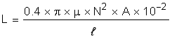
Equation 13. GUID-B410A391-8AF8-4E68-8235-7DF7C564713C-low.gif

where

  • µ is core permeability
  • N is the number of turns
  • A is the cross sectional area
  • l is the mean magnetic path length

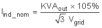
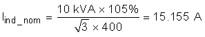
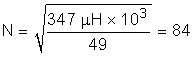
The starting point for evaluating a solution to the variables in Equation 13 is to determine a valid core material and subsequent permeability. The core manufacturer typically has a range of suitable materials with selection criteria based on the design inductance and the inductor current. For this design, the nominal inductor current (with an overload factor of 105%) is defined as:

Equation 14. GUID-2EE51A1A-59B2-49EE-9367-4A0169AE2BFF-low.gif
Equation 15. GUID-079213DC-CD8D-4DBD-B5AD-08D11E2DBE89-low.gif

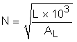
Using a selection guide for a toroidal inductor core manufacturer, at 347 µH, the core permeability comes to 26 µH. The core also provides a value for the inductance factor, AL, which enables a quick path to selecting the number of turns.

Equation 16. GUID-951BFE34-4E3A-4EEE-9800-7E45FE0377A3-low.gif
Equation 17. GUID-4A71B165-62BC-4489-8AF2-56BDA53E6747-low.gif

One last piece of information required for the inductor design is the winding wire size. This size is easily computed using the nominal inductor current rating. Using copper, with a current carrying density of 4 A/mm, this inductor requires a cross sectional area of:

Equation 18. GUID-2C676A44-B86B-4820-9E48-42B03479DBAB-low.gif

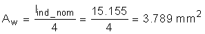
This area is an equivalent to American Wire Gauge #12, which has a cross sectional area of 3.309 mm2. This slight derating is acceptable because the switching current allows a smaller gauge to be used when compared to a static DC bias current. For this inductor, flat winding is used to increase surface area for cooling and decrease potential skin depth effects.

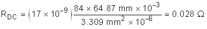
Using the overall design of the core, with the flat 12 AWG winding, the total length of each winding is determined to be 64.87 mm. At this point, the DC resistance of the inductor can be calculated using Pouillet's Law:

Equation 19. GUID-AC64E007-2E85-4FB7-B6EA-42E7E2F75896-low.gif
Equation 20. GUID-88CC5432-B4D1-487A-AA7F-15E7D755C465-low.gif

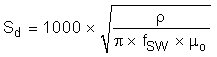
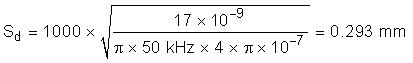
To determine the AC resistance, first calculate the skin depth at the inverter switching frequency:

Equation 21. GUID-ECAF6DEF-0626-4886-AB6A-AEE70CF6852E-low.gif
Equation 22. GUID-9B8C6F7F-3AE8-4554-B147-D724C0885BD0-low.gif

RAC is then determined by RDC, Sd, and Ss, which is the equivalent square conductor width.

Equation 23. GUID-74B07036-C6BD-4875-B4C2-545438299C74-low.gif

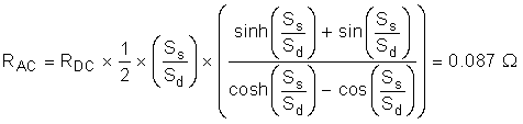
This determination of RAC helps determine total system losses.