JAJU510H March   2018  – December 2022


  1.   概要
  2.   リソース
  3.   特長
  4.   アプリケーション
  5.   5
  6. 1System Description
    1. 1.1 Key System Specifications
  7. 2System Overview
    1. 2.1 Block Diagram
    2. 2.2 Highlighted Products
      1. 2.2.1  UCC21710
      2. 2.2.2  UCC5320
      3. 2.2.3  TMS320F28379D
      4. 2.2.4  AMC1305M05
      5. 2.2.5  OPA4340
      6. 2.2.6  LM76003
      7. 2.2.7  PTH08080W
      8. 2.2.8  TLV1117
      9. 2.2.9  OPA350
      10. 2.2.10 UCC14240
    3. 2.3 System Design Theory
      1. 2.3.1 Three-Phase T-Type Inverter
        1. 2.3.1.1 Architecture Overview
        2. 2.3.1.2 LCL Filter Design
        3. 2.3.1.3 Inductor Design
        4. 2.3.1.4 SiC MOSFETs Selection
        5. 2.3.1.5 Loss Estimations
        6. 2.3.1.6 Thermal Considerations
      2. 2.3.2 Voltage Sensing
      3. 2.3.3 Current Sensing
      4. 2.3.4 System Power Supplies
        1. 2.3.4.1 Main Input Power Conditioning
        2. 2.3.4.2 Isolated Bias Supplies
      5. 2.3.5 Gate Drivers
        1. 2.3.5.1 1200-V SiC MOSFETs
        2. 2.3.5.2 650-V SiC MOSFETs
        3. 2.3.5.3 Gate Driver Bias Supply
      6. 2.3.6 Control Design
        1. 2.3.6.1 Current Loop Design
        2. 2.3.6.2 PFC DC Bus Voltage Regulation Loop Design
  8. 3Hardware, Software, Testing Requirements, and Test Results
    1. 3.1 Required Hardware and Software
      1. 3.1.1 Hardware
        1. 3.1.1.1 Test Hardware Required
        2. 3.1.1.2 Microcontroller Resources Used on the Design
        3. 3.1.1.3 F28377D, F28379D Control-Card Settings
      2. 3.1.2 Software
        1. 3.1.2.1 Getting Started With Firmware
          1. 3.1.2.1.1 Opening the CCS project
          2. 3.1.2.1.2 Digital Power SDK Software Architecture
          3. 3.1.2.1.3 Interrupts and Lab Structure
          4. 3.1.2.1.4 Building, Loading and Debugging the Firmware
        2. 3.1.2.2 Protection Scheme
        3. 3.1.2.3 PWM Switching Scheme
        4. 3.1.2.4 ADC Loading
    2. 3.2 Testing and Results
      1. 3.2.1 Lab 1
      2. 3.2.2 Testing Inverter Operation
        1. 3.2.2.1 Lab 2
        2. 3.2.2.2 Lab 3
        3. 3.2.2.3 Lab 4
      3. 3.2.3 Testing PFC Operation
        1. 3.2.3.1 Lab 5
        2. 3.2.3.2 Lab 6
        3. 3.2.3.3 Lab 7
      4. 3.2.4 Test Setup for Efficiency
      5. 3.2.5 Test Results
        1. 3.2.5.1 PFC Mode - 230 VRMS, 400 V L-L
          1. 3.2.5.1.1 PFC Start-up – 230 VRMS, 400 L-L AC Voltage
          2. 3.2.5.1.2 Steady State Results at 230 VRMS, 400 V L-L - PFC Mode
          3. 3.2.5.1.3 Efficiency and THD Results at 220 VRMS, 50 Hz – PFC Mode
          4. 3.2.5.1.4 Transient Test With Step Load Change
        2. 3.2.5.2 PFC Mode - 120 VRMS, 208 V L-L
          1. 3.2.5.2.1 Steady State Results at 120 VRMS, 208 V-L-L - PFC Mode
          2. 3.2.5.2.2 Efficiency and THD Results at 120 VRMS - PFC Mode
        3. 3.2.5.3 Inverter Mode
          1. 3.2.5.3.1 Inverter Closed Loop Results
          2. 3.2.5.3.2 Efficiency and THD Results - Inverter Mode
          3. 3.2.5.3.3 Inverter - Transient Test
      6. 3.2.6 Open Loop Inverter Test Results
  9. 4Design Files
    1. 4.1 Schematics
    2. 4.2 Bill of Materials
    3. 4.3 PCB Layout Recommendations
      1. 4.3.1 Layout Prints
    4. 4.4 Altium Project
    5. 4.5 Gerber Files
    6. 4.6 Assembly Drawings
  10. 5Trademarks
  11. 6About the Authors
  12. 7Revision History

Current Loop Design

For the inverter filter shown in Figure 2-45, using KCL and KVL Equation 49 can be written.

GUID-20210222-CA0I-H5V4-NXNS-TPQJNLWK0TZ1-low.gif Figure 2-45 Inverter Model
Equation 35. GUID-20210223-CA0I-ZHDM-Q6QD-W9P7NRPM4D4V-low.gif

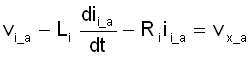
Upon re-arranging, Equation 49 can be written as Equation 36:

Equation 36. GUID-20210223-CA0I-BC8X-TVSF-TZK0XV1DRFH7-low.gif

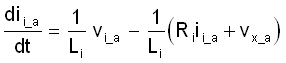
Similarly on another node, using KCL and KVL, Equation 37 can be written as Equation 37:

Equation 37. GUID-20210223-CA0I-321L-GWRS-G0FTVSWRRPRD-low.gif

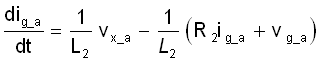
Assuming Rf is negligible Equation 38 can be written for the capacitor voltage:

Equation 38. GUID-20210223-CA0I-NDZ5-Q97K-CSV7WRRWWRGS-low.gif

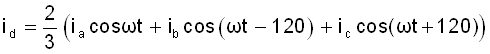
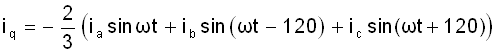
Typically a synchronous reference frame control is designed, where a dq rotating reference frame at grid frequency speed, and oriented such that the d axis is aligned to the grid voltage vector is used. Using basic trigonometric identities, id and iq can be written as Equation 39 and Equation 40.

Equation 39. GUID-20210223-CA0I-PBJ8-P3Z9-FN7TJX7ZQ94L-low.gif
Equation 40. GUID-20210223-CA0I-CXS8-VZGB-6DMSMT5SGN6Q-low.gif

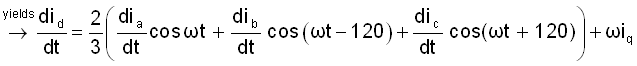
Taking the derivative, and using the partial derivative theorem, Equation 41 is written:

Equation 41. GUID-20210223-CA0I-KCFW-M9LD-KPLHQS1PDXTQ-low.gifGUID-20210223-CA0I-JN8J-WWRV-KZ4DGF80BNKJ-low.gif

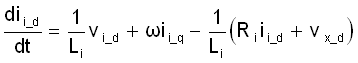
The following state equations can be written:

Equation 42. GUID-20210223-CA0I-SMFX-FBSW-PXDFMHQNG9L1-low.gif
Equation 43. GUID-20210223-CA0I-SGVM-QJX9-DP1VVX6QHG0C-low.gif

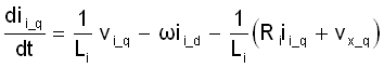
Hence, using these equations, and substituting in Equation 44:

Equation 44. GUID-20210223-CA0I-691P-VTTP-FMFHRVWL9KTL-low.gif

Taking the Laplace function on the previous equations:

Equation 45. GUID-20210223-CA0I-DLGM-CTHX-2R89ZLFG6XG3-low.gif

When written in control diagram format, this looks like the following. Feedforward elements are added to remove additional sources of disturbances and errors in the model, two feedforward elements are added,

  1. For the coupling term from the other axis in synchronous frame
  2. For the output grid voltage

The diagram is drawn as shown in Figure 2-46.
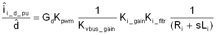
GUID-20210222-CA0I-QTRV-FLGM-1QKDDR2GLMJL-low.gif

where:

  • i*i_d is the current reference
  • Ki_gain is the current sense scalar which is one over max current sense
  • Ki_fltr is the filter that is connected on the current sense path. current sense scalar which is one over max current sense
  • Kvbus_gain is the voltage sense scalar for the bus, which is one over max voltage sensed
  • Kvg_gain is the voltage sense scalar for the grid voltage, which is one over max voltage sensed
Figure 2-46 Id Current Loop Model
GUID-20210222-CA0I-ML1W-3LBX-LBDKJ3V69BZ8-low.gif 
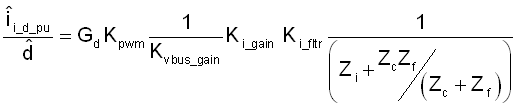
Figure 2-47 Iq Current Loop Model

With the feedforward elements, the small signal model can be written as Equation 46(Note: Separate scaling factors are applied to bus voltage and grid voltage due to the differences in the sensing range.):

Equation 46. GUID-20210223-CA0I-K2SL-Z0XD-FPLJ55KFSDPH-low.gif

In the case of an LCL filter, the following can be assumed as a simplified model as in Equation 47:

Equation 47. GUID-20210223-CA0I-TKKT-RTSV-HKVZVDFBQDGM-low.gif

The current loop plant is compared with the SFRA measured data for the current loop as illustrated in Figure 2-48.

GUID-20210223-CA0I-FDZZ-RWV0-ZSGDH4T87B0L-low.png Figure 2-48 Current Loop Plant Frequency Response Modelled vs Measured

Equation 48 represents the compensator designed for the closed-loop operation:

Equation 48. GUID-20210223-CA0I-BT1C-6T85-XVTV0N6ZWZRK-low.gif

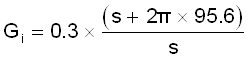
With which the open loop plot in Figure 2-49 is achieved, gives roughly > 1-kHz bandwidth in the Id and Iq loop.

GUID-20210223-CA0I-HCGM-TMCW-LDVQ3TKJ0ZDQ-low.png Figure 2-49 Current Loop, Open Loop Response Modelled vs Measured