JAJU510H March   2018  – December 2022


  1.   概要
  2.   リソース
  3.   特長
  4.   アプリケーション
  5.   5
  6. 1System Description
    1. 1.1 Key System Specifications
  7. 2System Overview
    1. 2.1 Block Diagram
    2. 2.2 Highlighted Products
      1. 2.2.1  UCC21710
      2. 2.2.2  UCC5320
      3. 2.2.3  TMS320F28379D
      4. 2.2.4  AMC1305M05
      5. 2.2.5  OPA4340
      6. 2.2.6  LM76003
      7. 2.2.7  PTH08080W
      8. 2.2.8  TLV1117
      9. 2.2.9  OPA350
      10. 2.2.10 UCC14240
    3. 2.3 System Design Theory
      1. 2.3.1 Three-Phase T-Type Inverter
        1. 2.3.1.1 Architecture Overview
        2. 2.3.1.2 LCL Filter Design
        3. 2.3.1.3 Inductor Design
        4. 2.3.1.4 SiC MOSFETs Selection
        5. 2.3.1.5 Loss Estimations
        6. 2.3.1.6 Thermal Considerations
      2. 2.3.2 Voltage Sensing
      3. 2.3.3 Current Sensing
      4. 2.3.4 System Power Supplies
        1. 2.3.4.1 Main Input Power Conditioning
        2. 2.3.4.2 Isolated Bias Supplies
      5. 2.3.5 Gate Drivers
        1. 2.3.5.1 1200-V SiC MOSFETs
        2. 2.3.5.2 650-V SiC MOSFETs
        3. 2.3.5.3 Gate Driver Bias Supply
      6. 2.3.6 Control Design
        1. 2.3.6.1 Current Loop Design
        2. 2.3.6.2 PFC DC Bus Voltage Regulation Loop Design
  8. 3Hardware, Software, Testing Requirements, and Test Results
    1. 3.1 Required Hardware and Software
      1. 3.1.1 Hardware
        1. 3.1.1.1 Test Hardware Required
        2. 3.1.1.2 Microcontroller Resources Used on the Design
        3. 3.1.1.3 F28377D, F28379D Control-Card Settings
      2. 3.1.2 Software
        1. 3.1.2.1 Getting Started With Firmware
          1. 3.1.2.1.1 Opening the CCS project
          2. 3.1.2.1.2 Digital Power SDK Software Architecture
          3. 3.1.2.1.3 Interrupts and Lab Structure
          4. 3.1.2.1.4 Building, Loading and Debugging the Firmware
        2. 3.1.2.2 Protection Scheme
        3. 3.1.2.3 PWM Switching Scheme
        4. 3.1.2.4 ADC Loading
    2. 3.2 Testing and Results
      1. 3.2.1 Lab 1
      2. 3.2.2 Testing Inverter Operation
        1. 3.2.2.1 Lab 2
        2. 3.2.2.2 Lab 3
        3. 3.2.2.3 Lab 4
      3. 3.2.3 Testing PFC Operation
        1. 3.2.3.1 Lab 5
        2. 3.2.3.2 Lab 6
        3. 3.2.3.3 Lab 7
      4. 3.2.4 Test Setup for Efficiency
      5. 3.2.5 Test Results
        1. 3.2.5.1 PFC Mode - 230 VRMS, 400 V L-L
          1. 3.2.5.1.1 PFC Start-up – 230 VRMS, 400 L-L AC Voltage
          2. 3.2.5.1.2 Steady State Results at 230 VRMS, 400 V L-L - PFC Mode
          3. 3.2.5.1.3 Efficiency and THD Results at 220 VRMS, 50 Hz – PFC Mode
          4. 3.2.5.1.4 Transient Test With Step Load Change
        2. 3.2.5.2 PFC Mode - 120 VRMS, 208 V L-L
          1. 3.2.5.2.1 Steady State Results at 120 VRMS, 208 V-L-L - PFC Mode
          2. 3.2.5.2.2 Efficiency and THD Results at 120 VRMS - PFC Mode
        3. 3.2.5.3 Inverter Mode
          1. 3.2.5.3.1 Inverter Closed Loop Results
          2. 3.2.5.3.2 Efficiency and THD Results - Inverter Mode
          3. 3.2.5.3.3 Inverter - Transient Test
      6. 3.2.6 Open Loop Inverter Test Results
  9. 4Design Files
    1. 4.1 Schematics
    2. 4.2 Bill of Materials
    3. 4.3 PCB Layout Recommendations
      1. 4.3.1 Layout Prints
    4. 4.4 Altium Project
    5. 4.5 Gerber Files
    6. 4.6 Assembly Drawings
  10. 5Trademarks
  11. 6About the Authors
  12. 7Revision History
Interrupts and Lab Structure

The project consists of two ISRs (ISR1 and ISR2) with ISR1 being the fastest and non-nestable ISR. ISR1 is reserved for the control loop and the PWM update. ISR1 is triggered by the PRIM_LEG1_PWM_BASE → EPWM_INT_TBCTR_U_CMPC event.

ISR2 is triggered by CPU Timer INT which is initiated by an overflow on CPU timer. It is used to run housekeeping functions such as doing a running average on the currents and voltage signals to remove noise and running the slew rate function for commanded references.
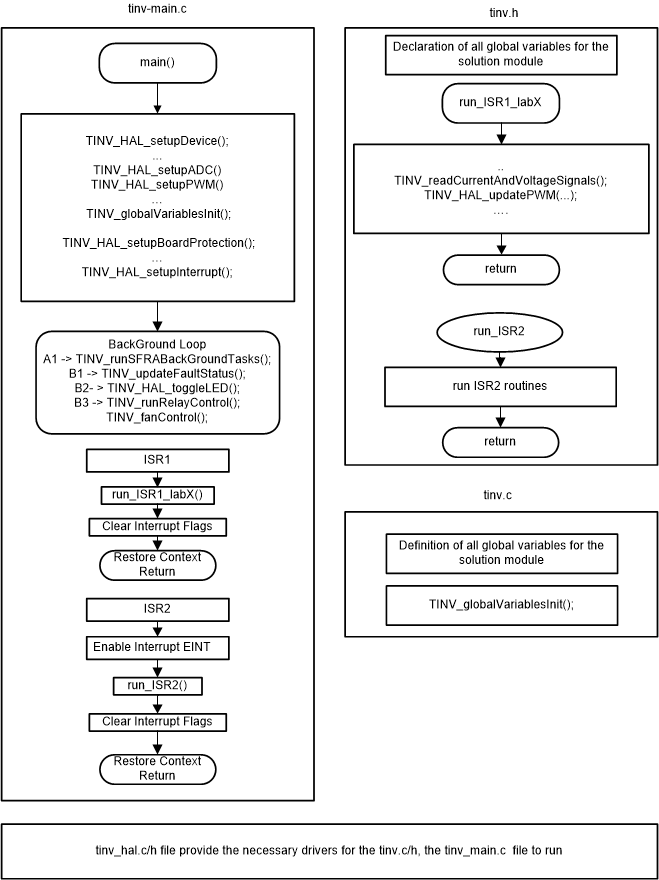
GUID-20210222-CA0I-LFPL-JM1N-TDGM1CQ95D3S-low.gifFigure 3-1 Software Flow Diagram

The software of this reference design is organized in seven labs, Table 3-3 lists the labs and how they have been tested. All the labs can be run on the C28x Main CPU or the Control Law Accelerator.

Table 3-3 Overview of Labs to Test Reference Design
LAB NUMBERDESCRIPTIONCOMMENTSTEST ENVIRONMENT
1INV: PWM and ADC checkTest the PWM driver, ISR structure and execution rate, can be run on a control card. Unit test protection mechanisms. Test ADC mapping and reading of conversion data.Control Card
2INV: Open loop checkPWM Check, ADC check, Protection Check, inverter mode DC bus connected and resistive star network as loadControl Card + Power Stage Hardware
3INV: Closed Current Loop, Resistive load connected at ACControl Card + Power Stage Hardware
4INV: Closed Current Loop, Grid connected test inverter modeControl Card +

Emulated power stage under Hardware In-the Loop

5PFC: Three phase AC source , Resistive load at DC, open Loop check
  1. Check if the vGridRms, iGridRms, vBus meas are correct
  2. Check if PLL is locked.
Control Card + Power Stage Hardware
6PFC: Closed Current Loop, Resistive load connected at DC, three phase AC ?Control Card + Power Stage Hardware
7PFC: Closed Voltage loop + Current Loop , Resistive load connected at DC, three phase AC ?Control Card + Power Stage Hardware