JAJU510H March   2018  – December 2022


  1.   概要
  2.   リソース
  3.   特長
  4.   アプリケーション
  5.   5
  6. 1System Description
    1. 1.1 Key System Specifications
  7. 2System Overview
    1. 2.1 Block Diagram
    2. 2.2 Highlighted Products
      1. 2.2.1  UCC21710
      2. 2.2.2  UCC5320
      3. 2.2.3  TMS320F28379D
      4. 2.2.4  AMC1305M05
      5. 2.2.5  OPA4340
      6. 2.2.6  LM76003
      7. 2.2.7  PTH08080W
      8. 2.2.8  TLV1117
      9. 2.2.9  OPA350
      10. 2.2.10 UCC14240
    3. 2.3 System Design Theory
      1. 2.3.1 Three-Phase T-Type Inverter
        1. 2.3.1.1 Architecture Overview
        2. 2.3.1.2 LCL Filter Design
        3. 2.3.1.3 Inductor Design
        4. 2.3.1.4 SiC MOSFETs Selection
        5. 2.3.1.5 Loss Estimations
        6. 2.3.1.6 Thermal Considerations
      2. 2.3.2 Voltage Sensing
      3. 2.3.3 Current Sensing
      4. 2.3.4 System Power Supplies
        1. 2.3.4.1 Main Input Power Conditioning
        2. 2.3.4.2 Isolated Bias Supplies
      5. 2.3.5 Gate Drivers
        1. 2.3.5.1 1200-V SiC MOSFETs
        2. 2.3.5.2 650-V SiC MOSFETs
        3. 2.3.5.3 Gate Driver Bias Supply
      6. 2.3.6 Control Design
        1. 2.3.6.1 Current Loop Design
        2. 2.3.6.2 PFC DC Bus Voltage Regulation Loop Design
  8. 3Hardware, Software, Testing Requirements, and Test Results
    1. 3.1 Required Hardware and Software
      1. 3.1.1 Hardware
        1. 3.1.1.1 Test Hardware Required
        2. 3.1.1.2 Microcontroller Resources Used on the Design
        3. 3.1.1.3 F28377D, F28379D Control-Card Settings
      2. 3.1.2 Software
        1. 3.1.2.1 Getting Started With Firmware
          1. 3.1.2.1.1 Opening the CCS project
          2. 3.1.2.1.2 Digital Power SDK Software Architecture
          3. 3.1.2.1.3 Interrupts and Lab Structure
          4. 3.1.2.1.4 Building, Loading and Debugging the Firmware
        2. 3.1.2.2 Protection Scheme
        3. 3.1.2.3 PWM Switching Scheme
        4. 3.1.2.4 ADC Loading
    2. 3.2 Testing and Results
      1. 3.2.1 Lab 1
      2. 3.2.2 Testing Inverter Operation
        1. 3.2.2.1 Lab 2
        2. 3.2.2.2 Lab 3
        3. 3.2.2.3 Lab 4
      3. 3.2.3 Testing PFC Operation
        1. 3.2.3.1 Lab 5
        2. 3.2.3.2 Lab 6
        3. 3.2.3.3 Lab 7
      4. 3.2.4 Test Setup for Efficiency
      5. 3.2.5 Test Results
        1. 3.2.5.1 PFC Mode - 230 VRMS, 400 V L-L
          1. 3.2.5.1.1 PFC Start-up – 230 VRMS, 400 L-L AC Voltage
          2. 3.2.5.1.2 Steady State Results at 230 VRMS, 400 V L-L - PFC Mode
          3. 3.2.5.1.3 Efficiency and THD Results at 220 VRMS, 50 Hz – PFC Mode
          4. 3.2.5.1.4 Transient Test With Step Load Change
        2. 3.2.5.2 PFC Mode - 120 VRMS, 208 V L-L
          1. 3.2.5.2.1 Steady State Results at 120 VRMS, 208 V-L-L - PFC Mode
          2. 3.2.5.2.2 Efficiency and THD Results at 120 VRMS - PFC Mode
        3. 3.2.5.3 Inverter Mode
          1. 3.2.5.3.1 Inverter Closed Loop Results
          2. 3.2.5.3.2 Efficiency and THD Results - Inverter Mode
          3. 3.2.5.3.3 Inverter - Transient Test
      6. 3.2.6 Open Loop Inverter Test Results
  9. 4Design Files
    1. 4.1 Schematics
    2. 4.2 Bill of Materials
    3. 4.3 PCB Layout Recommendations
      1. 4.3.1 Layout Prints
    4. 4.4 Altium Project
    5. 4.5 Gerber Files
    6. 4.6 Assembly Drawings
  10. 5Trademarks
  11. 6About the Authors
  12. 7Revision History

LM76003

The LM76002/LM76003 regulator is an easy-to-use synchronous step-down DC/DC converter capable of driving up to 2.5 A (LM76002) or 3.5 A (LM76003) of load current from an input up to 60 V. The LM76002/LM76003 provides exceptional efficiency and output accuracy in a very small solution size. Peak current-mode control is employed. Additional features such as adjustable switching frequency, synchronization, FPWM option, power-good flag, precision enable, adjustable soft start, and tracking provide both flexible and easy-to-use solutions for a wide range of applications. Automatic frequency foldback at light load and optional external bias improve efficiency. This device requires few external components and has a pinout designed for simple PCB layout with best-in-class EMI (CISPR22) and thermal performance. Protection features include thermal shutdown, input UVLO, cycle-by-cycle current limit, and short-circuit protection. The LM76002/LM76003 device is available in the WQFN 30-pin leadless package with wettable flanks.

  • Integrated synchronous rectification
  • Input voltage: 3.5 V to 60 V (65 V maximum)
  • Output current:
    • LM76002: 2.5 A
    • LM76003: 3.5 A
  • Output voltage: 1 V to 95% VIN
  • 15-µA quiescent current in regulation
  • Wide voltage conversion range:
    • tON-MIN = 65 ns (typical)
    • tOFF-MIN = 95 ns (typical)
  • System-level features:
    • Synchronization to external clock
    • Power-good flag
    • Precision enable
    • Adjustable soft start (6.3 ms default)
    • Voltage tracking capability
  • Pin-selectable FPWM operation
  • High-efficiency at light-load architecture (PFM)
  • Protection features:
    • Cycle-by-cycle current limit
    • Short-circuit protection with hiccup mode
    • Overtemperature thermal shutdown protection
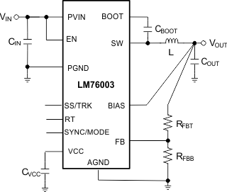
GUID-092476B5-435F-4EAC-9167-AD5E0AA653F3-low.gifFigure 2-7 LM76003 Simplified Schematic