JAJU510H March   2018  – December 2022


  1.   概要
  2.   リソース
  3.   特長
  4.   アプリケーション
  5.   5
  6. 1System Description
    1. 1.1 Key System Specifications
  7. 2System Overview
    1. 2.1 Block Diagram
    2. 2.2 Highlighted Products
      1. 2.2.1  UCC21710
      2. 2.2.2  UCC5320
      3. 2.2.3  TMS320F28379D
      4. 2.2.4  AMC1305M05
      5. 2.2.5  OPA4340
      6. 2.2.6  LM76003
      7. 2.2.7  PTH08080W
      8. 2.2.8  TLV1117
      9. 2.2.9  OPA350
      10. 2.2.10 UCC14240
    3. 2.3 System Design Theory
      1. 2.3.1 Three-Phase T-Type Inverter
        1. 2.3.1.1 Architecture Overview
        2. 2.3.1.2 LCL Filter Design
        3. 2.3.1.3 Inductor Design
        4. 2.3.1.4 SiC MOSFETs Selection
        5. 2.3.1.5 Loss Estimations
        6. 2.3.1.6 Thermal Considerations
      2. 2.3.2 Voltage Sensing
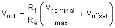
      3. 2.3.3 Current Sensing
      4. 2.3.4 System Power Supplies
        1. 2.3.4.1 Main Input Power Conditioning
        2. 2.3.4.2 Isolated Bias Supplies
      5. 2.3.5 Gate Drivers
        1. 2.3.5.1 1200-V SiC MOSFETs
        2. 2.3.5.2 650-V SiC MOSFETs
        3. 2.3.5.3 Gate Driver Bias Supply
      6. 2.3.6 Control Design
        1. 2.3.6.1 Current Loop Design
        2. 2.3.6.2 PFC DC Bus Voltage Regulation Loop Design
  8. 3Hardware, Software, Testing Requirements, and Test Results
    1. 3.1 Required Hardware and Software
      1. 3.1.1 Hardware
        1. 3.1.1.1 Test Hardware Required
        2. 3.1.1.2 Microcontroller Resources Used on the Design
        3. 3.1.1.3 F28377D, F28379D Control-Card Settings
      2. 3.1.2 Software
        1. 3.1.2.1 Getting Started With Firmware
          1. 3.1.2.1.1 Opening the CCS project
          2. 3.1.2.1.2 Digital Power SDK Software Architecture
          3. 3.1.2.1.3 Interrupts and Lab Structure
          4. 3.1.2.1.4 Building, Loading and Debugging the Firmware
        2. 3.1.2.2 Protection Scheme
        3. 3.1.2.3 PWM Switching Scheme
        4. 3.1.2.4 ADC Loading
    2. 3.2 Testing and Results
      1. 3.2.1 Lab 1
      2. 3.2.2 Testing Inverter Operation
        1. 3.2.2.1 Lab 2
        2. 3.2.2.2 Lab 3
        3. 3.2.2.3 Lab 4
      3. 3.2.3 Testing PFC Operation
        1. 3.2.3.1 Lab 5
        2. 3.2.3.2 Lab 6
        3. 3.2.3.3 Lab 7
      4. 3.2.4 Test Setup for Efficiency
      5. 3.2.5 Test Results
        1. 3.2.5.1 PFC Mode - 230 VRMS, 400 V L-L
          1. 3.2.5.1.1 PFC Start-up – 230 VRMS, 400 L-L AC Voltage
          2. 3.2.5.1.2 Steady State Results at 230 VRMS, 400 V L-L - PFC Mode
          3. 3.2.5.1.3 Efficiency and THD Results at 220 VRMS, 50 Hz – PFC Mode
          4. 3.2.5.1.4 Transient Test With Step Load Change
        2. 3.2.5.2 PFC Mode - 120 VRMS, 208 V L-L
          1. 3.2.5.2.1 Steady State Results at 120 VRMS, 208 V-L-L - PFC Mode
          2. 3.2.5.2.2 Efficiency and THD Results at 120 VRMS - PFC Mode
        3. 3.2.5.3 Inverter Mode
          1. 3.2.5.3.1 Inverter Closed Loop Results
          2. 3.2.5.3.2 Efficiency and THD Results - Inverter Mode
          3. 3.2.5.3.3 Inverter - Transient Test
      6. 3.2.6 Open Loop Inverter Test Results
  9. 4Design Files
    1. 4.1 Schematics
    2. 4.2 Bill of Materials
    3. 4.3 PCB Layout Recommendations
      1. 4.3.1 Layout Prints
    4. 4.4 Altium Project
    5. 4.5 Gerber Files
    6. 4.6 Assembly Drawings
  10. 5Trademarks
  11. 6About the Authors
  12. 7Revision History

Current Sensing

Critical to attaining a closed-loop control system is accurate current measurement of the inverter. In this design, current measurement is done at two locations with different sensing technologies. The first location is on the grid output using shunt resistors. Because the output is high voltage and the controller needs to remain isolated, the AMC1306M05 reinforced modulator is used to measure the resistor voltage drop. To keep system losses low, the AMC1306M05 has a ±50-mV input range. When compared to other devices with a typical input range of ±250 mV, the total power loss across the shunt is significantly reduced.

Sizing the shunt resistor for this design is a trade-off between sensing accuracy and power dissipation. A 0.002-Ω shunt provides a ±50-mV output signal at the approximate ±25-A output inverter but also only generates 0.5 W of heat at full load. When choosing an actual device, select a high accuracy value to eliminate the need to calibrate each sensor path.

The voltage across the shunt resistor is fed into the AMC1306M05 sigma-delta modulator, which generates the sigma-delta stream that is decoded by the SDFM demodulator present on the C2000™ MCU. The clock for the modulator is generated from the eCAP peripheral on the C2000 MCU, and the AMC1306M05 data is decided using the built-in SDFM modulator.

GUID-86A1D2B1-4EC6-4E51-83C6-3EFEDD227C78-low.gifFigure 2-37 Isolated Shunt Sensing With AMC1305M05

The second location is a Hall-effect sensor, which is used to sense the current through the inductor. The Hall-effect sensor has a built-in offset, and the range is different than what ADC can measure. Therefore, the voltage is scaled to match the ADC range using the circuit shown in Figure 2-39 and Equation 33. Of note here, the OPA4340 is used over the OPA4350 in the voltage sense path due to the lower bandwidth of the former. The low bandwidth helps to reduce accidental amplification of switching noise that can be picked up by long traces in the PCB.

Figure 2-38 Isolated Hall Effect Current Sensing
Figure 2-39 Hall Effect Sensor Matching
Equation 33. GUID-A393B531-E11B-41E5-899A-7C13A03EBDDB-low.gif