SNOAA35D April 2023 – December 2023 LM2901 , LM2901B , LM2901B-Q1 , LM2903 , LM2903-Q1 , LM2903B , LM2903B-Q1 , LM339 , LM339-N , LM393 , LM393-N , LM393B , LM397 , TL331 , TL331-Q1 , TL331B
- 1
- Application Design Guidelines for LM339, LM393, TL331 Family Comparators Including the New B-versions
- Trademarks
- 1 Devices Covered in Application Note
- 2 The New TL331B, TL391B, LM339B, LM393B, LM2901B and LM2903B B Versions
-
3 Input Considerations
- 3.1 Input Stage Schematic – The Classic LM339 Family
- 3.2 Input Stage Schematic - New B Devices
- 3.3 Differences Between the Classic and B Die Devices
- 3.4 Input Voltage Range
- 3.5 Input Voltage Range vs. Common Mode Voltage Range
- 3.6 Reason for Input Range Headroom Limitation
- 3.7 Input Voltage Range Feature
- 3.8 Negative Input Voltages
- 3.9 Power-Up Behavior
- 3.10 Capacitors and Hysteresis
- 3.11 Output to Input Cross-Talk
- 4 Output Stage Considerations
- 5 Power Supply Considerations
- 6 General Comparator Usage
- 7 PSPICE and TINA TI Models
- 8 Conclusion
- 9 Related Documentation
- 10Revision History
4.1 Output VOL and IOL
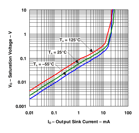
A critical graph for the output is the Output voltage vs Output Current graph, shown in Figure 4-1. From this graph, the output Low voltage can be determined from the expected sinking load current.
 Figure 4-1 Typical Output Low (Saturation) Voltage vs Output Sinking Current
The graph also shows the current limit, where the output voltage sharply inflects upwards in the 10-20mA region. This region must be avoided as the specified minimum short circuit current is only 6mA (typically 12-16mA) and can vary across devices, lots and temperature. TI recommends sinking currents of less than 5mA.
This graph must also be used to determine the pull-up resistor value needed for a desired output low voltage.
For example, if a 3.3kΩ resistor is used on a 3.3 V pull-up voltage, the resulting current is 1mA when sinking. From the graph, 1mA will result in a worst-case (125°C) VOL voltage of 90mV. However, if a 330 ohm pull-up resistor is used, the output low voltage is now 350mV, and is also uncomfortably close to the current limit.