SNOAA35D April 2023 – December 2023 LM2901 , LM2901B , LM2901B-Q1 , LM2903 , LM2903-Q1 , LM2903B , LM2903B-Q1 , LM339 , LM339-N , LM393 , LM393-N , LM393B , LM397 , TL331 , TL331-Q1 , TL331B
- 1
- Application Design Guidelines for LM339, LM393, TL331 Family Comparators Including the New B-versions
- Trademarks
- 1 Devices Covered in Application Note
- 2 The New TL331B, TL391B, LM339B, LM393B, LM2901B and LM2903B B Versions
-
3 Input Considerations
- 3.1 Input Stage Schematic – The Classic LM339 Family
- 3.2 Input Stage Schematic - New B Devices
- 3.3 Differences Between the Classic and B Die Devices
- 3.4 Input Voltage Range
- 3.5 Input Voltage Range vs. Common Mode Voltage Range
- 3.6 Reason for Input Range Headroom Limitation
- 3.7 Input Voltage Range Feature
- 3.8 Negative Input Voltages
- 3.9 Power-Up Behavior
- 3.10 Capacitors and Hysteresis
- 3.11 Output to Input Cross-Talk
- 4 Output Stage Considerations
- 5 Power Supply Considerations
- 6 General Comparator Usage
- 7 PSPICE and TINA TI Models
- 8 Conclusion
- 9 Related Documentation
- 10Revision History
3.8.3.1 Simple Resistor and Diode Clamp
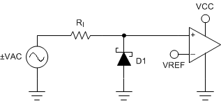
In cases where a negative input voltage cannot be avoided, such as ringing from inductive sources of bipolar outputs or from direct coupled sensors, a current limiting resistor in series with the input can limit the current to a safe level, as shown in Figure 3-6. The diode must be a Schottky type for lowest forward voltage.
The resistor must be calculated to limit the current to 1mA or less at the highest expected voltage. A rule of thumb is 1kΩ per volt of expected over-voltage. So if the maximum expected negative voltage is -5V, the resistor must be at least 5kΩ or greater. This resistance can be part of the divider or other resistive input network. A similar resistance can be added to the other input for bias current cancellation. The size of the resistor is a compromise between minimum clamp current, bias current error and minimum added delay for AC signals.
 Figure 3-6 Series Resistor And Diode Negative Voltage Protection
If the resistor value is too high, interaction with the comparator input bias current and leakage currents of the diode can cause shifts in the threshold points. High resistor values can also cause delays in AC signals due to the time constant of the input and stray capacitance and the resistor.
If the resistor value is too low, the forward voltage of the diode will increase due to the higher clamp current, as well as load-down the source while clamping. Lower values are better for AC signals due to the lower delay.
The disadvantage of this simple clamp approach is that the forward voltage of the diode can exceed the -300mV input limit, even when using low forward voltage Schottky type diode.
If large negative input voltages are expected, such as zero crossing detectors or input signals with inductive ringing, which require clamping the negative portion of the input signal, then a low ratio voltage divider must then be used. See Section 3.8.3.2.1.