SNOAA35D April 2023 – December 2023 LM2901 , LM2901B , LM2901B-Q1 , LM2903 , LM2903-Q1 , LM2903B , LM2903B-Q1 , LM339 , LM339-N , LM393 , LM393-N , LM393B , LM397 , TL331 , TL331-Q1 , TL331B
- 1
- Application Design Guidelines for LM339, LM393, TL331 Family Comparators Including the New B-versions
- Trademarks
- 1 Devices Covered in Application Note
- 2 The New TL331B, TL391B, LM339B, LM393B, LM2901B and LM2903B B Versions
-
3 Input Considerations
- 3.1 Input Stage Schematic – The Classic LM339 Family
- 3.2 Input Stage Schematic - New B Devices
- 3.3 Differences Between the Classic and B Die Devices
- 3.4 Input Voltage Range
- 3.5 Input Voltage Range vs. Common Mode Voltage Range
- 3.6 Reason for Input Range Headroom Limitation
- 3.7 Input Voltage Range Feature
- 3.8 Negative Input Voltages
- 3.9 Power-Up Behavior
- 3.10 Capacitors and Hysteresis
- 3.11 Output to Input Cross-Talk
- 4 Output Stage Considerations
- 5 Power Supply Considerations
- 6 General Comparator Usage
- 7 PSPICE and TINA TI Models
- 8 Conclusion
- 9 Related Documentation
- 10Revision History
6.1.2 Unused Comparator Input Connections
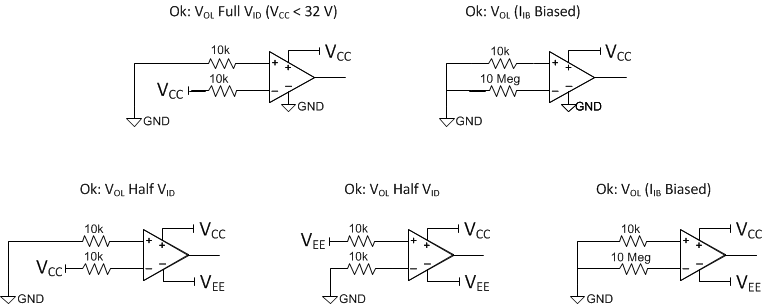
Occasionally applications will not need all the comparators in a dual or quad package. The unused channels must be connected in a way that is safe for the unused comparator and doesn’t affect the used comparators. The best connection method puts the comparator into the normal operation range and no inputs are connected directly to low impedance nodes. The output of the comparator must be left open and not connected.
 Figure 6-1 Best
Connections Practices for Single and Dual Supplies
Figure 6-1 Best
Connections Practices for Single and Dual SuppliesIncreasing the input resistor to 10 MΩ would ensure linear operation as the input bias current (Ib), which flows out of the input pin towards ground, would raise the non-inverting input voltage beyond the input offset voltage range. VOL Full VID is better suited for lower voltage applications as there is no reason to apply a large input voltage difference even though the comparator allows it. The VOL (IIB Biased) method uses the input bias current to raise the voltage on the inverting input. If used, place the 10-MΩ resistor close to the inverting input pin to reduce noise pickup. No inputs may be connected directly to low impedance nodes such as ground, VCC or VEE. VOH alternatives are also acceptable; just swap the input pins.
The next set of connections in Figure 6-2 is not recommended, but these configurations are not considered harmful methods of terminating unused channels. The VOH alternatives that swap the inputs are also not recommended methods of terminating unused channels.
 Figure 6-2 Less Than
Acceptable Connection Practices for Single and Dual Supplies
Figure 6-2 Less Than
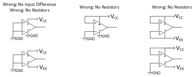
Acceptable Connection Practices for Single and Dual SuppliesThe last set of connections, shown in Figure 6-3, demonstrates improper setups that could cause output noise chatter or device damage if the GND pin were to ever become positive relative to the input pin.
 Figure 6-3 Potentially Harmful Connection Practices for Single and Dual Supplies