SNOAA35D April 2023 – December 2023 LM2901 , LM2901B , LM2901B-Q1 , LM2903 , LM2903-Q1 , LM2903B , LM2903B-Q1 , LM339 , LM339-N , LM393 , LM393-N , LM393B , LM397 , TL331 , TL331-Q1 , TL331B
- 1
- Application Design Guidelines for LM339, LM393, TL331 Family Comparators Including the New B-versions
- Trademarks
- 1 Devices Covered in Application Note
- 2 The New TL331B, TL391B, LM339B, LM393B, LM2901B and LM2903B B Versions
-
3 Input Considerations
- 3.1 Input Stage Schematic – The Classic LM339 Family
- 3.2 Input Stage Schematic - New B Devices
- 3.3 Differences Between the Classic and B Die Devices
- 3.4 Input Voltage Range
- 3.5 Input Voltage Range vs. Common Mode Voltage Range
- 3.6 Reason for Input Range Headroom Limitation
- 3.7 Input Voltage Range Feature
- 3.8 Negative Input Voltages
- 3.9 Power-Up Behavior
- 3.10 Capacitors and Hysteresis
- 3.11 Output to Input Cross-Talk
- 4 Output Stage Considerations
- 5 Power Supply Considerations
- 6 General Comparator Usage
- 7 PSPICE and TINA TI Models
- 8 Conclusion
- 9 Related Documentation
- 10Revision History
3.8 Negative Input Voltages
The LM339 family does not like negative input voltage on any I/O pins, and this is mentioned several times in the data sheets. The LM339 family is built using a junction-isolated die process, wherein all the individual on-die devices are electrically separated from the substrate by a reversed PN junction. This can be thought of as a reversed diode under every circuit node to a common die substrate. These junctions are commonly referred to as the Body Diode or Substrate Diode. For this junction isolation to function properly, the substrate must be maintained at the most negative potential. The die substrate is electrically tied to the GND pin, and thus the GND pin must be at the most negative circuit potential for proper operation.
If any pin is brought more negative than the GND pin (substrate), these various substrate junctions and parasitic transistors will start to conduct. Reverse currents now flow in paths that were not designed for current flow and this can cause parasitic devices to appear, leading to malfunctions, or worse, latch-up if the input current is high enough.
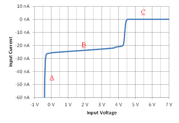
Figure 3-5 shows the input current of the input pin with a +5 V supply, sweeping the input from -1 V to +7 V. Noticeable nanoamp currents will start to flow when the input is at -0.3 V, and will increase to several tens of milliamps as the diodes start to conduct.
 Figure 3-5 Classic Input Pin I/V Curve with 5 V Supply
Section A shows the substrate diode knee starting to conduct at -400mV, with the subsequent increase in reverse current as the negative input voltage is increased.
Section B shows the normal operating Input Bias Current from 0 V up to 3.5 V. The gray zone can be seen as the current heads up towards zero after 4 V.
Section C shows the near zero (picoamp) bias currents as the input devices are reversed and cut off and no base current flows.
When the LM339 Family was originally designed in the early 70's, Electrostatic Discharge (ESD) damage was not as prevalent due to the high breakdown voltages of these older processes, so dedicated ESD protection structures were not included in the LM339 family. Without dedicated ESD structures, there is not a defined current path for reverse currents back to the GND pin. The new B devices do have dedicated ESD structures added to the inputs and output pins for more robust ESD performance.