SBAS999A June 2019 – January 2021 ADS125H01
PRODUCTION DATA
- 1 Features
- 2 Applications
- 3 Description
- 4 Revision History
- 5 Device Comparison Table
- 6 Pin Configuration and Functions
- 7 Specifications
- 8 Parameter Measurement Information
-
9 Detailed Description
- 9.1 Overview
- 9.2 Functional Block Diagram
- 9.3 Feature Description
- 9.4 Device Functional Modes
- 9.5 Programming
- 9.6
Register Map
- 9.6.1 Device Identification (ID) Register (address = 00h) [reset = 4xh]
- 9.6.2 Main Status (STATUS0) Register (address = 01h) [reset = 01h]
- 9.6.3 Mode 0 (MODE0) Register (address = 02h) [reset = 24h]
- 9.6.4 Mode 1 (MODE1) Register (address = 03h) [reset = 01h]
- 9.6.5 Reserved (RESERVED) Register (address = 04h) [reset = 00h]
- 9.6.6 Mode 3 (MODE3) Register (address = 05h) [reset = 00h]
- 9.6.7 Reference Configuration (REF) Register (address = 06h) [reset = 05h]
- 9.6.8 Offset Calibration (OFCALx) Registers (address = 07h, 08h, 09h) [reset = 00h, 00h, 00h]
- 9.6.9 Full-Scale Calibration (FSCALx) Registers (address = 0Ah, 0Bh, 0Ch) [reset = 00h, 00h, 40h]
- 9.6.10 Reserved (RESERVED) Register (address = 0Dh) [reset = FFh]
- 9.6.11 Reserved (RESERVED) Register (address = 0Eh) [reset = 00h]
- 9.6.12 Reserved (RESERVED) Register (address = 0Fh) [reset = 00h]
- 9.6.13 MODE4 (MODE4) Register (address = 10h) [reset = 50h]
- 9.6.14 PGA Alarm (STATUS1) Register (address = 11h) [reset = xxh]
- 9.6.15 Status 2 (STATUS2) Register (address = 12h) [reset = 0xh]
- 10Application and Implementation
- 11Power Supply Recommendations
- 12Layout
- 13Device and Documentation Support
- 14Mechanical, Packaging, and Orderable Information
Package Options
Mechanical Data (Package|Pins)
- RHB|32
Thermal pad, mechanical data (Package|Pins)
- RHB|32
Orderable Information
9.3.3 Programmable Gain Amplifier (PGA)
The PGA is a low-noise, programmable gain (attenuation), CMOS differential-input, differential-output amplifier. The PGA operates in gain or attenuation mode depending on the selected gain. Typically, the PGA is programmed for gain when the expected input signal voltage is ≤ VREF and is programmed for attenuation when the expected input signal voltage is ≥ VREF.
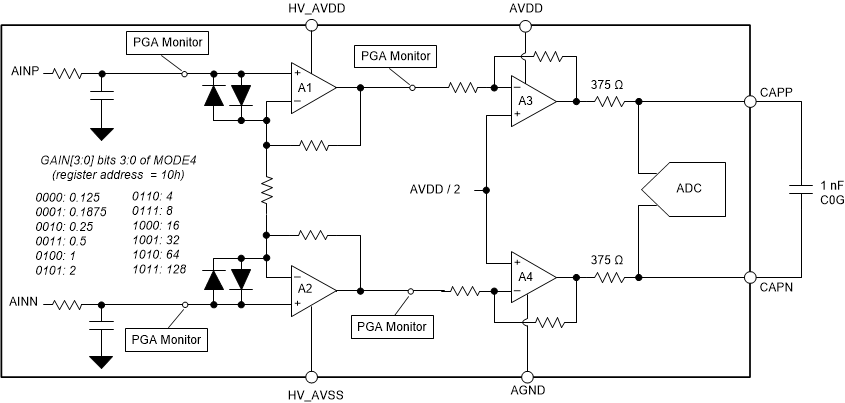
Figure 9-1 shows the block diagram of the PGA.
 Figure 9-1 PGA Block Diagram
The signal inputs are RC filtered to reduce sensitivity to radio frequency interference (RFI) and electromagnetic interference (EMI). The first PGA stage is a high input-impedance, noninverting differential amplifier (amplifiers A1 and A2) and provides gain. Inverse-parallel connected diodes across the inputs of A1 and A2 clamp the amplifier input voltage if they are driven out-of-range. If the amplifier is out-of-range, the diodes can conduct, resulting in current flow through the analog input pins. High dV/dt input signals, such as those generated from the switching of a multiplexer, can lead to transient turn-on of the clamp diodes. In some cases, an RC filter at the PGA inputs may be necessary to limit the dV/dt of the signal to prevent the clamp diodes from turning on.
The second stage (amplifiers A3 and A4) is an inverting, differential amplifier. This stage provides attenuation of high-amplitude signal levels. The common-mode voltage of this stage is AVDD / 2. The second stage drives the modulator input of the ADC and is also connected to the CAPP and CAPN pins. An external 1-nF capacitor filters the modulator input sample pulses and also provides the antialias filter for the ADC. Place the capacitor close to the pins using short, direct traces. Avoid running clock traces or other digital traces underneath or in the vicinity of these pins. Gain is programmed by the GAIN[3:0] bits of the MODE 4 register.
Monitors verify the voltage headroom of the PGA input and output nodes. See the Section 9.3.3.2 section for details.