SLVSFF3C December 2021 – October 2022 DRV8328
PRODUCTION DATA
- 1 Features
- 2 Applications
- 3 Description
- 4 Revision History
- 5 Device Comparison Table
- 6 Pin Configuration and Functions
- 7 Specification
-
8 Detailed Description
- 8.1 Overview
- 8.2 Functional Block Diagram
- 8.3
Feature Description
- 8.3.1 Three BLDC Gate Drivers
- 8.3.2 AVDD Linear Voltage Regulator
- 8.3.3 Pin Diagrams
- 8.3.4 Gate Driver Shutdown Sequence (DRVOFF)
- 8.3.5
Gate Driver Protective Circuits
- 8.3.5.1 PVDD Supply Undervoltage Lockout (PVDD_UV)
- 8.3.5.2 AVDD Power on Reset (AVDD_POR)
- 8.3.5.3 GVDD Undervoltage Lockout (GVDD_UV)
- 8.3.5.4 BST Undervoltage Lockout (BST_UV)
- 8.3.5.5 MOSFET VDS Overcurrent Protection (VDS_OCP)
- 8.3.5.6 VSENSE Overcurrent Protection (SEN_OCP)
- 8.3.5.7 Thermal Shutdown (OTSD)
- 8.4 Device Functional Modes
-
9 Application and Implementation
- 9.1 Application Information
- 9.2
Typical Application
- 9.2.1
Three Phase Brushless-DC Motor Control
- 9.2.1.1
Detailed Design Procedure
- 9.2.1.1.1 Motor Voltage
- 9.2.1.1.2 Bootstrap Capacitor and GVDD Capacitor Selection
- 9.2.1.1.3 Gate Drive Current
- 9.2.1.1.4 Gate Resistor Selection
- 9.2.1.1.5 System Considerations in High Power Designs
- 9.2.1.1.6 Dead Time Resistor Selection
- 9.2.1.1.7 VDSLVL Selection
- 9.2.1.1.8 AVDD Power Losses
- 9.2.1.1.9 Power Dissipation and Junction Temperature Losses
- 9.2.1.1
Detailed Design Procedure
- 9.2.2 Application Curves
- 9.2.1
Three Phase Brushless-DC Motor Control
- 10Power Supply Recommendations
- 11Layout
- 12Device and Documentation Support
- 13Mechanical, Packaging, and Orderable Information
Package Options
Mechanical Data (Package|Pins)
- RUY|28
Thermal pad, mechanical data (Package|Pins)
Orderable Information
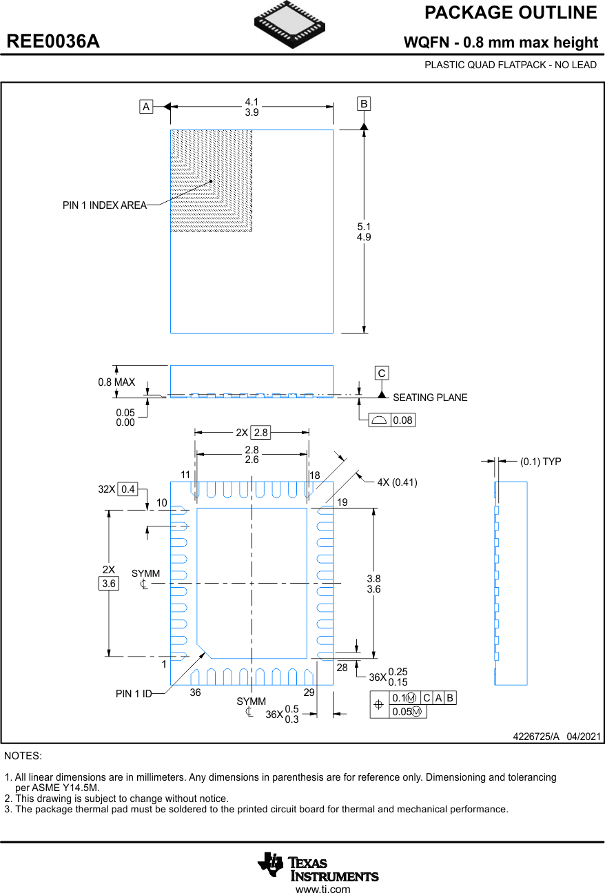
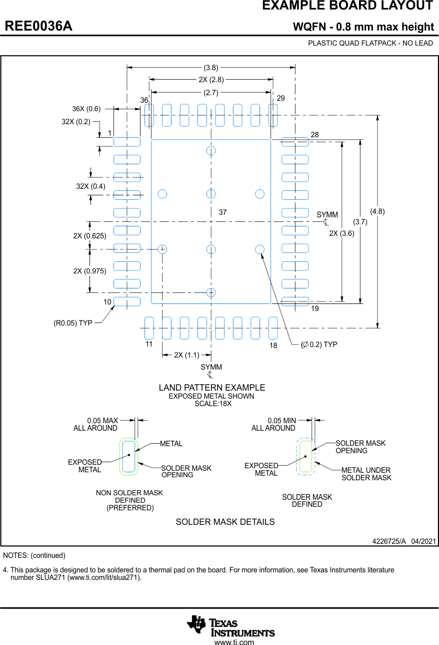
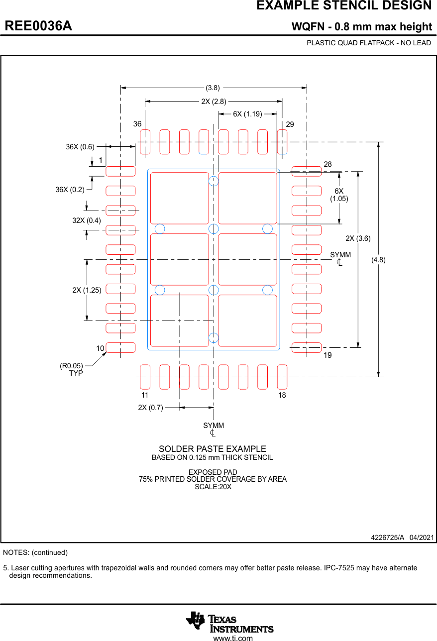
13 Mechanical, Packaging, and Orderable Information
The following pages include mechanical, packaging, and orderable information. This information is the most current data available for the designated devices. This data is subject to change without notice and revision of this document. For browser-based versions of this data sheet, refer to the left-hand navigation.