SLOSE54C June 2020 – July 2022 DRV8428
PRODUCTION DATA
- 1 Features
- 2 Applications
- 3 Description
- 4 Revision History
- 5 Pin Configuration and Functions
- 6 Specifications
-
7 Detailed Description
- 7.1 Overview
- 7.2 Functional Block Diagram
- 7.3
Feature Description
- 7.3.1 Stepper Motor Driver Current Ratings
- 7.3.2 PWM Motor Drivers
- 7.3.3 Microstepping Indexer
- 7.3.4 Controlling VREF with an MCU DAC
- 7.3.5 Current Regulation, Off-time and Decay Modes
- 7.3.6 Linear Voltage Regulators
- 7.3.7 Logic Level, tri-level, quad-level and seven-level Pin Diagrams
- 7.3.8 Protection Circuits
- 7.4 Device Functional Modes
- 8 Application and Implementation
- 9 Power Supply Recommendations
- 10Layout
- 11Device and Documentation Support
- 12Mechanical, Packaging, and Orderable Information
Package Options
Mechanical Data (Package|Pins)
Thermal pad, mechanical data (Package|Pins)
Orderable Information
7.3.7.1 EN/nFAULT Pin
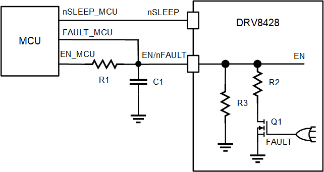
The EN/nFAULT pin is used to enable the driver and also used for fault reporting. Figure 7-15 shows the internal circuitry connected to the EN/nFAULT pin. When the pin is intended to be used for both enabling the driver and fault reporting, the external R-C has to be connected. When the pin is only intended for enabling and disabling the driver, the R-C is not required.
To enable the H-bridges, the pin must be driven high. Floating the pin or connecting the pin to ground forces the bridge to become high-Z.
When a fault is detected, EN/nFAULT pin is forced low by turning on Q1 - which discharges the capacitor C1. The H-bridges are disabled when the voltage on the EN/nFAULT pin falls below the VIL threshold. The bridges stay disabled till the fault condition is removed or a second MCU pin directly applies a voltage higher than VIH to the EN/nFAULT pin. Thereafter, Q1 is turned off and C1 charges back through the resistor R1.
The typical delay from EN/nFAULT rising edge to the enabling the H-bridges is 100 µs. The time constant of R1 * C1 must be less than 20 µs. Typical values of the resistors R2 and R3 are 16 kΩ and 2 MΩ respectively. When the EN/nFAULT pin is permanently tied high, a fault will cause additional leakage current due to Q1 being ON.
 Figure 7-15 EN/nFAULT Pin