SLOSE79B August 2022 – October 2023 DRV8462
PRODUCTION DATA
- 1
- 1 Features
- 2 Applications
- 3 Description
- 4 Revision History
- 5 Pin Configuration and Functions
- 6 Specifications
-
7 Detailed Description
- 7.1 Overview
- 7.2 Functional Block Diagram
- 7.3
Feature Description
- 7.3.1 Interface of Operation
- 7.3.2 Stepper Motor Driver Current Ratings
- 7.3.3 PWM Motor Drivers
- 7.3.4 Microstepping Indexer
- 7.3.5 Indexer Output
- 7.3.6 Automatic Microstepping Mode
- 7.3.7 Custom Microstepping Table
- 7.3.8 Current Regulation
- 7.3.9 Internal Reference Voltage
- 7.3.10 Standstill Power Saving Mode
- 7.3.11 Current Regulation Decay Modes
- 7.3.12 Current Sensing with External Resistor
- 7.3.13 Silent step decay mode
- 7.3.14 Auto-torque Dynamic Current Adjustment
- 7.3.15 Charge Pump
- 7.3.16 Linear Voltage Regulator
- 7.3.17 VCC Voltage Supply
- 7.3.18 Logic Level, Tri-Level and Quad-Level Pin Diagrams
- 7.3.19 Spread spectrum
- 7.3.20
Protection Circuits
- 7.3.20.1 VM Undervoltage Lockout
- 7.3.20.2 VCP Undervoltage Lockout (CPUV)
- 7.3.20.3 Logic Supply Power on Reset (POR)
- 7.3.20.4 Overcurrent Protection (OCP)
- 7.3.20.5 Stall Detection
- 7.3.20.6 Open-Load Detection (OL)
- 7.3.20.7 Overtemperature Warning (OTW)
- 7.3.20.8 Thermal Shutdown (OTSD)
- 7.3.20.9 Supply voltage sensing
- 7.3.20.10 nFAULT Output
- 7.3.20.11 Fault Condition Summary
- 7.3.21 Device Functional Modes
- 7.4 Programming
- 7.5
Register Maps
- 7.5.1 Status Registers
- 7.5.2
Control Registers
- 7.5.2.1 CTRL1 (address = 0x04) [Default = 0Fh]
- 7.5.2.2 CTRL2 (address = 0x05) [Default = 06h]
- 7.5.2.3 CTRL3 (address = 0x06) [Default = 38h]
- 7.5.2.4 CTRL4 (address = 0x07) [Default = 49h]
- 7.5.2.5 CTRL5 (address = 0x08) [Default = 03h]
- 7.5.2.6 CTRL6 (address = 0x09) [Default = 20h]
- 7.5.2.7 CTRL7 (address = 0x0A) [Default = FFh]
- 7.5.2.8 CTRL8 (address = 0x0B) [Default = 0Fh]
- 7.5.2.9 CTRL9 (address = 0x0C) [Default = 10h]
- 7.5.2.10 CTRL10 (address = 0x0D) [Default = 80h]
- 7.5.2.11 CTRL11 (address = 0x0E) [Default = FFh]
- 7.5.2.12 CTRL12 (address = 0x0F) [Default = 20h]
- 7.5.2.13 CTRL13 (address = 0x10) [Default = 10h]
- 7.5.2.14 CTRL14 (address = 0x3C) [Default = 58h]
- 7.5.3 Indexer Registers
- 7.5.4
Custom Microstepping Registers
- 7.5.4.1 CUSTOM_CTRL1 (address = 0x16) [Default = 00h]
- 7.5.4.2 CUSTOM_CTRL2 (address = 0x17) [Default = 00h]
- 7.5.4.3 CUSTOM_CTRL3 (address = 0x18) [Default = 00h]
- 7.5.4.4 CUSTOM_CTRL4 (address = 0x19) [Default = 00h]
- 7.5.4.5 CUSTOM_CTRL5 (address = 0x1A) [Default = 00h]
- 7.5.4.6 CUSTOM_CTRL6 (address = 0x1B) [Default = 00h]
- 7.5.4.7 CUSTOM_CTRL7 (address = 0x1C) [Default = 00h]
- 7.5.4.8 CUSTOM_CTRL8 (address = 0x1D) [Default = 00h]
- 7.5.4.9 CUSTOM_CTRL9 (address = 0x1E) [Default = 00h]
- 7.5.5
Auto torque Registers
- 7.5.5.1 ATQ_CTRL1 (address = 0x1F) [Default = 00h]
- 7.5.5.2 ATQ_CTRL2 (address = 0x20) [Default = 00h]
- 7.5.5.3 ATQ_CTRL3 (address = 0x21) [Default = 00h]
- 7.5.5.4 ATQ_CTRL4 (address = 0x22) [Default = 20h]
- 7.5.5.5 ATQ_CTRL5 (address = 0x23) [Default = 00h]
- 7.5.5.6 ATQ_CTRL6 (address = 0x24) [Default = 00h]
- 7.5.5.7 ATQ_CTRL7 (address = 0x25) [Default = 00h]
- 7.5.5.8 ATQ_CTRL8 (address = 0x26) [Default = 00h]
- 7.5.5.9 ATQ_CTRL9 (address = 0x27) [Default = 00h]
- 7.5.5.10 ATQ_CTRL10 (address = 0x28) [Default = 08h]
- 7.5.5.11 ATQ_CTRL11 (address = 0x29) [Default = 0Ah]
- 7.5.5.12 ATQ_CTRL12 (address = 0x2A) [Default = FFh]
- 7.5.5.13 ATQ_CTRL13 (address = 0x2B) [Default = 05h]
- 7.5.5.14 ATQ_CTRL14 (address = 0x2C) [Default = 0Fh]
- 7.5.5.15 ATQ_CTRL15 (address = 0x2D) [Default = 00h]
- 7.5.5.16 ATQ_CTRL16 (address = 0x2E) [Default = FFh]
- 7.5.5.17 ATQ_CTRL17 (address = 0x2F) [Default = 00h]
- 7.5.5.18 ATQ_CTRL18 (address = 0x30) [Default = 00h]
- 7.5.6 Silent Step Registers
- 8 Application and Implementation
- 9 Thermal Considerations
- 10Power Supply Recommendations
- 11Layout
- 12Device and Documentation Support
- 13Mechanical, Packaging, and Orderable Information
Package Options
Mechanical Data (Package|Pins)
Thermal pad, mechanical data (Package|Pins)
- DDW|44
Orderable Information
7.3.11.3 Smart tune Dynamic Decay
The smart tunes are advanced current regulation schemes compared to traditional mixed decay modes. Smart tune helps the stepper motor driver adjust the decay scheme based on changes in operating factors such as:
- Motor winding resistance and inductance
- Motor aging
- Motor dynamic speed and load
- Motor supply voltage variation
- Motor back-EMF difference on rising and falling steps
- Step transitions
- Low-current versus high-current dI/dt
The DRV8462 supports two different smart tune schemes - smart tune Dynamic Decay and smart tune Ripple Control.
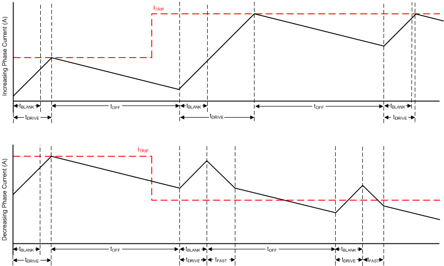
 Figure 7-16 Smart tune Dynamic Decay Mode
Smart tune Dynamic Decay dynamically adjusts the fast decay percentage of the total mixed decay time. This eliminates the need for motor decay tuning by automatically determining the best mixed decay setting that results in the lowest ripple and best performance for the motor.
The fast decay percentage is optimized iteratively each PWM cycle. If the motor current overshoots the target ITRIP level, then the mixed decay mode becomes more aggressive (by increasing fast decay percentage) on the next cycle to prevent loss of current regulation. If a long drive time must occur to reach the target ITRIP level, the decay mode becomes less aggressive (by reducing fast decay percentage) on the next cycle to operate with less ripple. On falling steps, smart tune Dynamic Decay automatically switches to fast decay to reach the next step quickly.