SNVSB29C October   2018  – June 2021 LM5143-Q1

PRODUCTION DATA  

  1. Features
  2. Applications
  3. Description
  4. Revision History
  5. Description (continued)
  6. Pin Configuration and Functions
    1. 6.1 Wettable Flanks
  7. Specifications
    1. 7.1 Absolute Maximum Ratings
    2. 7.2 ESD Ratings
    3. 7.3 Recommended Operating Conditions
    4. 7.4 Thermal Information
    5. 7.5 Electrical Characteristics
    6. 7.6 Switching Characteristics
    7. 7.7 Typical Characteristics
  8. Detailed Description
    1. 8.1 Overview
    2. 8.2 Functional Block Diagram
    3. 8.3 Feature Description
      1. 8.3.1  Input Voltage Range (VIN)
      2. 8.3.2  High-Voltage Bias Supply Regulator (VCC, VCCX, VDDA)
      3. 8.3.3  Enable (EN1, EN2)
      4. 8.3.4  Power Good Monitor (PG1, PG2)
      5. 8.3.5  Switching Frequency (RT)
      6. 8.3.6  Clock Synchronization (DEMB)
      7. 8.3.7  Synchronization Out (SYNCOUT)
      8. 8.3.8  Spread Spectrum Frequency Modulation (DITH)
      9. 8.3.9  Configurable Soft Start (SS1, SS2)
      10. 8.3.10 Output Voltage Setpoint (FB1, FB2)
      11. 8.3.11 Minimum Controllable On-Time
      12. 8.3.12 Error Amplifier and PWM Comparator (FB1, FB2, COMP1, COMP2)
      13. 8.3.13 Slope Compensation
      14. 8.3.14 Inductor Current Sense (CS1, VOUT1, CS2, VOUT2)
        1. 8.3.14.1 Shunt Current Sensing
        2. 8.3.14.2 Inductor DCR Current Sensing
      15. 8.3.15 Hiccup Mode Current Limiting (RES)
      16. 8.3.16 High-Side and Low-Side Gate Drivers (HO1/2, LO1/2, HOL1/2, LOL1/2)
      17. 8.3.17 Output Configurations (MODE, FB2)
        1. 8.3.17.1 Independent Dual-Output Operation
        2. 8.3.17.2 Single-Output Interleaved Operation
        3. 8.3.17.3 Single-Output Multiphase Operation
    4. 8.4 Device Functional Modes
      1. 8.4.1 Standby Modes
      2. 8.4.2 Diode Emulation Mode
      3. 8.4.3 Thermal Shutdown
  9. Application and Implementation
    1. 9.1 Application Information
      1. 9.1.1 Power Train Components
        1. 9.1.1.1 Buck Inductor
        2. 9.1.1.2 Output Capacitors
        3. 9.1.1.3 Input Capacitors
        4. 9.1.1.4 Power MOSFETs
        5. 9.1.1.5 EMI Filter
      2. 9.1.2 Error Amplifier and Compensation
    2. 9.2 Typical Applications
      1. 9.2.1 Design 1 – High Efficiency, Dual-Output Buck Regulator for Automotive Applications
        1. 9.2.1.1 Design Requirements
        2. 9.2.1.2 Detailed Design Procedure
          1. 9.2.1.2.1 Custom Design With WEBENCH® Tools
          2. 9.2.1.2.2 Custom Design With Excel Quickstart Tool
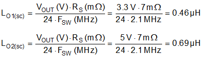
          3. 9.2.1.2.3 Inductor Calculation
          4. 9.2.1.2.4 Current-Sense Resistance
          5. 9.2.1.2.5 Output Capacitors
          6. 9.2.1.2.6 Input Capacitors
          7. 9.2.1.2.7 Compensation Components
        3. 9.2.1.3 Application Curves
      2. 9.2.2 Design 2 – Two-Phase, Single-Output Buck Regulator for Automotive ADAS Applications
        1. 9.2.2.1 Design Requirements
        2. 9.2.2.2 Detailed Design Procedures
        3. 9.2.2.3 Application Curves
  10. 10Power Supply Recommendations
  11. 11Layout
    1. 11.1 Layout Guidelines
      1. 11.1.1 Power Stage Layout
      2. 11.1.2 Gate-Drive Layout
      3. 11.1.3 PWM Controller Layout
      4. 11.1.4 Thermal Design and Layout
      5. 11.1.5 Ground Plane Design
    2. 11.2 Layout Example
  12. 12Device and Documentation Support
    1. 12.1 Device Support
      1. 12.1.1 Third-Party Products Disclaimer
      2. 12.1.2 Development Support
      3. 12.1.3 Custom Design With WEBENCH® Tools
    2. 12.2 Documentation Support
      1. 12.2.1 Related Documentation
        1. 12.2.1.1 PCB Layout Resources
        2. 12.2.1.2 Thermal Design Resources
    3. 12.3 Receiving Notification of Documentation Updates
    4. 12.4 Support Resources
    5. 12.5 Trademarks
    6. 12.6 Electrostatic Discharge Caution
    7. 12.7 Glossary
  13. 13Mechanical, Packaging, and Orderable Information

Package Options

Mechanical Data (Package|Pins)
Thermal pad, mechanical data (Package|Pins)
Orderable Information
Inductor Calculation
  1. Use Equation 33 to calculate the required buck inductance for each channel based on a 30% inductor ripple current at nominal input voltages.
    Equation 33. GUID-AEAB1393-8A5E-4032-AE7F-445A382B7D7F-low.gif
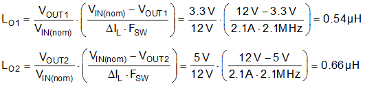
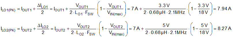
  2. Select a standard inductor value of 0.68 µH for both channels. Use Equation 34 to calculate the peak inductor currents at maximum steady-state input voltage. Subharmonic oscillation occurs with a duty cycle greater than 50% for peak current-mode control. For design simplification, the LM5143-Q1 has an internal slope compensation ramp proportional to the switching frequency that is added to the current sense signal to damp any tendency toward subharmonic oscillation.
    Equation 34. GUID-61EA760B-C761-4522-B734-E5935A339E1A-low.gif
  3. Based on Equation 10, use Equation 35 to cross-check the inductance to set a slope compensation equal to the ideal one times the inductor current downslope.
Equation 35. GUID-F17C17FC-E036-48FE-B339-BC91D880673A-low.gif