SNVSB29C October 2018 – June 2021 LM5143-Q1
PRODUCTION DATA
- 1 Features
- 2 Applications
- 3 Description
- 4 Revision History
- 5 Description (continued)
- 6 Pin Configuration and Functions
- 7 Specifications
-
8 Detailed Description
- 8.1 Overview
- 8.2 Functional Block Diagram
- 8.3
Feature Description
- 8.3.1 Input Voltage Range (VIN)
- 8.3.2 High-Voltage Bias Supply Regulator (VCC, VCCX, VDDA)
- 8.3.3 Enable (EN1, EN2)
- 8.3.4 Power Good Monitor (PG1, PG2)
- 8.3.5 Switching Frequency (RT)
- 8.3.6 Clock Synchronization (DEMB)
- 8.3.7 Synchronization Out (SYNCOUT)
- 8.3.8 Spread Spectrum Frequency Modulation (DITH)
- 8.3.9 Configurable Soft Start (SS1, SS2)
- 8.3.10 Output Voltage Setpoint (FB1, FB2)
- 8.3.11 Minimum Controllable On-Time
- 8.3.12 Error Amplifier and PWM Comparator (FB1, FB2, COMP1, COMP2)
- 8.3.13 Slope Compensation
- 8.3.14 Inductor Current Sense (CS1, VOUT1, CS2, VOUT2)
- 8.3.15 Hiccup Mode Current Limiting (RES)
- 8.3.16 High-Side and Low-Side Gate Drivers (HO1/2, LO1/2, HOL1/2, LOL1/2)
- 8.3.17 Output Configurations (MODE, FB2)
- 8.4 Device Functional Modes
-
9 Application and Implementation
- 9.1 Application Information
- 9.2 Typical Applications
- 10Power Supply Recommendations
- 11Layout
- 12Device and Documentation Support
- 13Mechanical, Packaging, and Orderable Information
Package Options
Mechanical Data (Package|Pins)
- RWG|40
Thermal pad, mechanical data (Package|Pins)
Orderable Information
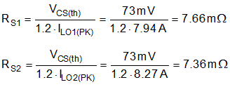
9.2.1.2.4 Current-Sense Resistance
- Calculate the current-sense resistance based on a maximum peak current capability of at least 20% higher than the peak inductor current at full load to provide sufficient margin during start-up and load-on transients. Calculate the current sense resistances using Equation 36.
Equation 36.
where
- VCS(th) is the 73-mV current limit threshold.
- Select a standard resistance value of 7 mΩ for both shunts. A 0508 footprint component with wide aspect ratio termination design provides 1-W power rating, low parasitic series inductance, and compact PCB layout. Carefully observe the Section 11.1 to make sure that noise and DC errors do not corrupt the differential current-sense voltages measured at [CS1, VOUT1] and [CS2, VOUT2].
- Place the shunt resistor close to the inductor.
- Use Kelvin-sense connections, and route the sense lines differentially from the shunt to the LM5143-Q1.
- The CS-to-output propagation delay (related to the current limit comparator, internal logic and power MOSFET gate drivers) causes the peak current to increase above the calculated current limit threshold. For a total propagation delay of tCS-DELAY of 40 ns, use Equation 37 to calculate the worst-case peak inductor current with the output shorted.
Equation 37.

- Based on this result, select an inductor for each channel with saturation current greater than 12 A across the full operating temperature range.