SNVSB29C October 2018 – June 2021 LM5143-Q1
PRODUCTION DATA
- 1 Features
- 2 Applications
- 3 Description
- 4 Revision History
- 5 Description (continued)
- 6 Pin Configuration and Functions
- 7 Specifications
-
8 Detailed Description
- 8.1 Overview
- 8.2 Functional Block Diagram
- 8.3
Feature Description
- 8.3.1 Input Voltage Range (VIN)
- 8.3.2 High-Voltage Bias Supply Regulator (VCC, VCCX, VDDA)
- 8.3.3 Enable (EN1, EN2)
- 8.3.4 Power Good Monitor (PG1, PG2)
- 8.3.5 Switching Frequency (RT)
- 8.3.6 Clock Synchronization (DEMB)
- 8.3.7 Synchronization Out (SYNCOUT)
- 8.3.8 Spread Spectrum Frequency Modulation (DITH)
- 8.3.9 Configurable Soft Start (SS1, SS2)
- 8.3.10 Output Voltage Setpoint (FB1, FB2)
- 8.3.11 Minimum Controllable On-Time
- 8.3.12 Error Amplifier and PWM Comparator (FB1, FB2, COMP1, COMP2)
- 8.3.13 Slope Compensation
- 8.3.14 Inductor Current Sense (CS1, VOUT1, CS2, VOUT2)
- 8.3.15 Hiccup Mode Current Limiting (RES)
- 8.3.16 High-Side and Low-Side Gate Drivers (HO1/2, LO1/2, HOL1/2, LOL1/2)
- 8.3.17 Output Configurations (MODE, FB2)
- 8.4 Device Functional Modes
-
9 Application and Implementation
- 9.1 Application Information
- 9.2 Typical Applications
- 10Power Supply Recommendations
- 11Layout
- 12Device and Documentation Support
- 13Mechanical, Packaging, and Orderable Information
Package Options
Mechanical Data (Package|Pins)
- RWG|40
Thermal pad, mechanical data (Package|Pins)
Orderable Information
8.3.16 High-Side and Low-Side Gate Drivers (HO1/2, LO1/2, HOL1/2, LOL1/2)
The LM5143-Q1 contains N-channel MOSFET gate drivers and an associated high-side level shifter to drive the external N-channel MOSFET. The high-side gate driver works in conjunction with an external bootstrap diode DBST and bootstrap capacitor CBST. See Figure 8-7. During the conduction interval of the low-side MOSFET, the SW voltage is approximately 0 V and CBST is charged from VCC through DBST. TI recommends a 0.1-μF ceramic capacitor connected with short traces between the applicable HB and SW pins.
The LO and HO outputs are controlled with an adaptive dead-time methodology so that both outputs (HO and LO) are never enabled at the same time, preventing cross conduction. When the controller commands LO to be enabled, the adaptive dead-time logic first disables HO and waits for the HO-SW voltage to drop below 2.5 V typical. LO is then enabled after a small delay (HO fall to LO rising delay). Similarly, the HO turnon is delayed until the LO voltage has dropped below 2.5 V. HO is then enabled after a small delay (LO falling to HO rising delay). This technique ensures adequate dead time for any size N-channel MOSFET component or parallel MOSFET configurations.
Caution is advised when adding series gate resistors, as this can decrease the effective dead time. Each of the high-side and low-side drivers has an independent driver source and sink output pins. This allows the user to adjust drive strength to optimize the switching losses for maximum efficiency and control the slew rate for reduced EMI signature. The selected N-channel high-side MOSFET determines the appropriate bootstrap capacitance values CBST in Figure 8-7 according to Equation 14.
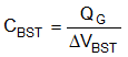
where
- QG is the total gate charge of the high-side MOSFET at the applicable gate drive voltage
- ΔVBST is the voltage variation of the high-side MOSFET driver after turnon
To determine CBST, choose ΔVBST so that the available gate drive voltage is not significantly impacted. An acceptable range of ΔVBST is 100 mV to 300 mV. The bootstrap capacitor must be a low-ESR ceramic capacitor, typically 0.1 µF. Use high-side and low-side MOSFETs with logic level gate threshold voltages.
 Figure 8-7 Integrated MOSFET Gate Drivers