SNVSBU3 March 2021 LP87702
PRODUCTION DATA
- 1 Features
- 2 Applications
- 3 Description
- 4 Revision History
- 5 Pin Configuration and Functions
- 6 Specifications
-
7 Detailed Description
- 7.1 Overview
- 7.2 Functional Block Diagram
- 7.3
Feature Descriptions
- 7.3.1 Step-Down DC/DC Converters
- 7.3.2 Boost Converter
- 7.3.3 Spread-Spectrum Mode
- 7.3.4 Sync Clock Functionality
- 7.3.5 Power-Up
- 7.3.6 Buck and Boost Control
- 7.3.7 Enable and Disable Sequences
- 7.3.8 Window Watchdog
- 7.3.9 Device Reset Scenarios
- 7.3.10 Diagnostics and Protection Features
- 7.3.11 OTP Error Correction
- 7.3.12 Operation of GPO Signals
- 7.3.13 Digital Signal Filtering
- 7.4 Device Functional Modes
- 7.5 Programming
- 7.6 Register Maps
- 8 Application and Implementation
- 9 Power Supply Recommendations
- 10Layout
- 11Device and Documentation Support
- 12Mechanical, Packaging, and Orderable Information
Package Options
Mechanical Data (Package|Pins)
- RHB|32
Thermal pad, mechanical data (Package|Pins)
- RHB|32
Orderable Information
7.3.8 Window Watchdog
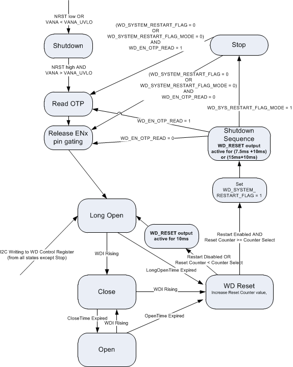
Figure 7-8 shows the LP87702 watchdog's operation (for an example, when the ENx pin is used for controlling power sequence and ENx pin is active).
WDI is the watchdog function input pin, and WD_RESET is the reset output. The WDI pin needs pulsed within a certain timing window to avoid a watchdog expiration. The minimum pulse width is 100 µs. The watchdog expiration always causes a reset pulse at WD_RESET output, otherwise the device behavior after watchdog expiration is programmable. WD_RESET output polarity and mode, push-pull or open drain, are also programmable.
Watchdog default settings are read from OTP during device start-up. Default settings in WD_CTRL_1 and WD_CTRL_2 register can be over-written through the I2C (as long as WD_LOCK bit is not set to 1). Writing WD_LOCK = 1 in WD_CTRL_2 register locks watchdog settings until NRST input is driven low, power cycle or register reset by SW_RESET.
Table 7-4 shows how the long open, close, and open window periods are independently programmable. The watchdog enters the WD Reset state when the long open or open window expires before the WDI input is received. Also, the watchdog enters the WD Reset when the WDI is received during close window. Long open period can be extended by a I2C write to WD_CTRL_1 or WD_CTRL_2 register; the register access initializes the long open counter and the long open period restarts (except in Stop mode).
LP87702 behavior after WD expiration is programmable:
- When WD_RESET_CNTR_SEL = 00, system restart is disabled and converters are maintained ON. WD_RESET pin is active for 10 ms. Watchdog returns to Long Open mode.
- When WD_RESET_CNTR_SEL = 01 (restart after first reset pulse), LP87702 performs shutdown sequence followed by start-up sequence so the converters are disabled and re-enabled according to the OTP programmed sequences. The device reloads OTP defaults when WD_EN_OTP_READ = 1 during start-up. Settings valid before shutdown are maintained when the WD_EN_OTP_READ = 0. WD_RESET output pin is active for a period of (10 ms + maximum shutdown delay). Maximum shutdown delay can be selected as 7.5 ms (SHUTDOWN_DELAY_SEL = 0) or 15 ms (SHUTDOWN_DELAY_SEL = 1). After the restart watchdog returns to Long Open mode.
- The status bit (WD_SYSTEM_RESTART_FLAG) is set to indicate that a system restart has happened. The status can be cleared by writing 1 to WD_CLR_SYSTEM_RESTART_FLAG. WD_RESET_CNTR_SEL can be set to 10 or 11 to select restart after 2 or 4 WD expirations, respectively. The current status of the reset counter is available in WD_RESET_CNTR_STATUS. The reset counter can be cleared by writing WD_CLR_RESET_CNTR to 1.
Watchdog settings in WD_CTRL_1 and WD_CTRL_2 registers are locked by setting the WD_LOCK bit. WD_SYSTEM_RESTART_FLAG and WD_RESET_CNTR_STATUS can be cleared even if WD_LOCK = 1.
Description above is for a case where ENx pin is used for controlling power sequence and ENx pin is active. Watchdog behavior can be slightly different depending on the OTP settings and the ENx pin state, which follows:
- When the ENx pin is used for controlling the power sequence and the ENx pin is not active, the shutdown sequence cannot be performed. WD_RESET pulse length is fixed 31 ms.
- There is no OTP defined power sequence when the ENx pins are not used for power sequence control, and all converters and GPOs are enabled through the I2C. WD expiration does not cause a converter disable or enable sequence even when the OTP settings for the watchdog enable restart. In this case WD_RESET pulse is 11 ms.
 Figure 7-8 Watchdog Operation
| CONTROL BIT | DEFAULT | VALUES |
|---|---|---|
| WD_LONG_OPEN_TIME | OTP | 00 – 200 ms 01 – 600 ms 10 – 2000 ms 11 – 5000 ms |
| WD_CLOSE_TIME | OTP | 00 – 10 ms 01 – 20 ms 10 – 50 ms 11 – 100 ms |