SNVSBU3 March 2021 LP87702
PRODUCTION DATA
- 1 Features
- 2 Applications
- 3 Description
- 4 Revision History
- 5 Pin Configuration and Functions
- 6 Specifications
-
7 Detailed Description
- 7.1 Overview
- 7.2 Functional Block Diagram
- 7.3
Feature Descriptions
- 7.3.1 Step-Down DC/DC Converters
- 7.3.2 Boost Converter
- 7.3.3 Spread-Spectrum Mode
- 7.3.4 Sync Clock Functionality
- 7.3.5 Power-Up
- 7.3.6 Buck and Boost Control
- 7.3.7 Enable and Disable Sequences
- 7.3.8 Window Watchdog
- 7.3.9 Device Reset Scenarios
- 7.3.10 Diagnostics and Protection Features
- 7.3.11 OTP Error Correction
- 7.3.12 Operation of GPO Signals
- 7.3.13 Digital Signal Filtering
- 7.4 Device Functional Modes
- 7.5 Programming
- 7.6 Register Maps
- 8 Application and Implementation
- 9 Power Supply Recommendations
- 10Layout
- 11Device and Documentation Support
- 12Mechanical, Packaging, and Orderable Information
Package Options
Mechanical Data (Package|Pins)
- RHB|32
Thermal pad, mechanical data (Package|Pins)
- RHB|32
Orderable Information
7.3.10.4.1 Output Power Limit
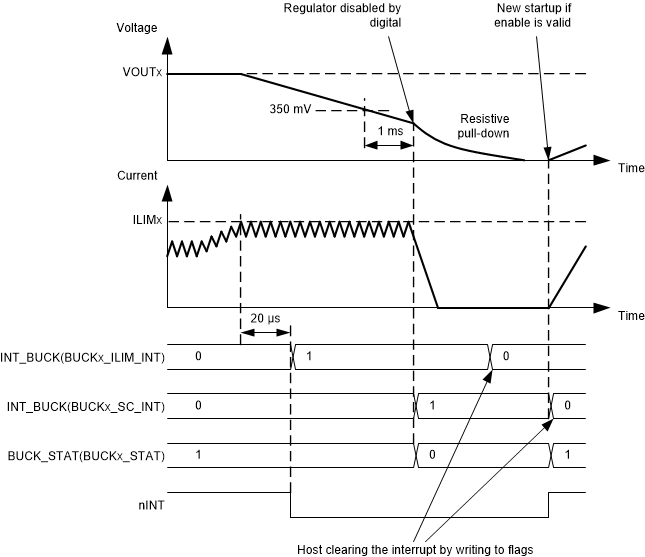
The buck converters have programmable output peak current limits. The limits are individually programmed for both converters with BUCKx_ILIM[2:0] bits. If the load current is increased so that the current limit is triggered, the converter continues to regulate to the limit current level (current peak regulation). The voltage may decrease if the load current is higher than limit current. If the current regulation continues for 20 µs, the LP87702 device sets the BUCKx_ILIM_INT bit and pulls the nINT pin low. The host processor can read the BUCKx_ILIM_STAT bits to see if the converter is still in peak current regulation mode. During startup or output voltage ramp (output voltage change has been programmed) no interrupt is generated.
If the load is so high that the output voltage decreases below a 350-mV level, the LP87702 device disables the converter and sets the BUCKx_SC_INT bit. The interrupt is cleared when the host processor writes 1 to BUCKx_SC_INT bit. Figure 7-12 shows the Buck overload situation.
 Figure 7-12 Buck Overload Situation
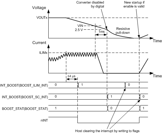
The boost converter has programmable output peak current limits. The limits are set with the BOOST_ILIM bits. If the load current is increased so that the current limit is triggered, the converter continues to regulate to the limit current level (current peak regulation). The voltage may decrease if the load current is higher than limit current. If the current regulation continues for 64 µs, the LP87702 device sets the BOOST_ILIM_INT bit and pulls the nINT pin low. The host processor can read the BOOST_ILIM_STAT bits to see if the converter is still in peak current regulation mode.
If the load is so high that the output voltage decreases 150 mV (typical) below the input voltage level, then the converter is disabled after 1 ms. If the output voltage decreases to 2.5 V, boost stops switching. After 1 ms the deglitch time boost is fully disabled and the interrupt BOOST_SC_INT bit is set. The interrupt is cleared when the host processor writes 1 to the BOOST_SC_INT bit. Figure 7-13 shows the Boost overload situation.
 Figure 7-13 Boost Overload Situation
The buck converters have a fixed current limit for negative output peak current (ILIM_NEG). When the negative coil current increases, it is limited below ILIM_NEG, the converter continues to operate and no interrupt is generated. The boost converter's negative peak current limit operation is similar and the limit value is 1.4 A (typical).