SNVSBU3 March   2021 LP87702

PRODUCTION DATA  

  1. Features
  2. Applications
  3. Description
  4. Revision History
  5. Pin Configuration and Functions
  6. Specifications
    1. 6.1 Absolute Maximum Ratings
    2. 6.2 ESD Ratings
    3. 6.3 Recommended Operating Conditions
    4. 6.4 Thermal Information
    5. 6.5 Electrical Characteristics
    6. 6.6 I2C Serial Bus Timing Parameters
    7. 6.7 Typical Characteristics
  7. Detailed Description
    1. 7.1 Overview
    2. 7.2 Functional Block Diagram
    3. 7.3 Feature Descriptions
      1. 7.3.1  Step-Down DC/DC Converters
        1. 7.3.1.1 Overview
        2. 7.3.1.2 Transition Between PWM and PFM Modes
        3. 7.3.1.3 Buck Converter Load Current Measurement
      2. 7.3.2  Boost Converter
      3. 7.3.3  Spread-Spectrum Mode
      4. 7.3.4  Sync Clock Functionality
      5. 7.3.5  Power-Up
      6. 7.3.6  Buck and Boost Control
        1. 7.3.6.1 Enabling and Disabling Converters
        2. 7.3.6.2 Changing Buck Output Voltage
      7. 7.3.7  Enable and Disable Sequences
      8. 7.3.8  Window Watchdog
      9. 7.3.9  Device Reset Scenarios
      10. 7.3.10 Diagnostics and Protection Features
        1. 7.3.10.1 Voltage Monitorings
        2. 7.3.10.2 Interrupts
        3. 7.3.10.3 Power-Good Information to Interrupt, PG0, and PG1 Pins
          1. 7.3.10.3.1 PGx Pin Gated (Unusual) Mode
          2. 7.3.10.3.2 PGx Pin Operation in Continuous Mode
          3. 7.3.10.3.3 Summary of PG0, PG1 Gated, and Continuous Operating Modes
        4. 7.3.10.4 Warning Interrupts for System Level Diagnostics
          1. 7.3.10.4.1 Output Power Limit
          2. 7.3.10.4.2 Thermal Warning
        5. 7.3.10.5 Protections Causing Converter Disable
          1. 7.3.10.5.1 Short-Circuit and Overload Protection
          2. 7.3.10.5.2 Overvoltage Protection
          3. 7.3.10.5.3 Thermal Shutdown
        6. 7.3.10.6 Protections Causing Device Power Down
          1. 7.3.10.6.1 Undervoltage Lockout
      11. 7.3.11 OTP Error Correction
      12. 7.3.12 Operation of GPO Signals
      13. 7.3.13 Digital Signal Filtering
    4. 7.4 Device Functional Modes
      1. 7.4.1 Modes of Operation
    5. 7.5 Programming
      1. 7.5.1 I2C-Compatible Interface
        1. 7.5.1.1 Data Validity
        2. 7.5.1.2 Start and Stop Conditions
        3. 7.5.1.3 Transferring Data
        4. 7.5.1.4 I2C-Compatible Chip Address
        5. 7.5.1.5 Auto Increment Feature
    6. 7.6 Register Maps
      1. 7.6.1 Register Descriptions
        1. 7.6.1.1 LP8770_map Registers
  8. Application and Implementation
    1. 8.1 Application Information
    2. 8.2 Typical Application
      1. 8.2.1 Design Requirements
      2. 8.2.2 Detailed Design Procedure
        1. 8.2.2.1 Application Components
          1. 8.2.2.1.1 Inductor Selection
          2. 8.2.2.1.2 Buck Input Capacitor Selection
          3. 8.2.2.1.3 Buck Output Capacitor Selection
          4. 8.2.2.1.4 Boost Input Capacitor Selection
          5. 8.2.2.1.5 Boost Output Capacitor Selection
          6. 8.2.2.1.6 Supply Filtering Components
      3. 8.2.3 Current Limit vs Maximum Output Current
      4. 8.2.4 Application Curves
  9. Power Supply Recommendations
  10. 10Layout
    1. 10.1 Layout Guidelines
    2. 10.2 Layout Example
  11. 11Device and Documentation Support
    1. 11.1 Third-Party Products Disclaimer
    2. 11.2 Receiving Notification of Documentation Updates
    3. 11.3 Support Resources
    4. 11.4 Trademarks
    5. 11.5 Electrostatic Discharge Caution
    6. 11.6 Glossary
  12. 12Mechanical, Packaging, and Orderable Information

Package Options

Mechanical Data (Package|Pins)
Thermal pad, mechanical data (Package|Pins)
Orderable Information

Changing Buck Output Voltage

The output voltage of BUCKx converter can be changed by writing to the BUCKx_VOUT register. The voltage change for buck converter is always slew-rate controlled, and the slew-rate is defined by the BUCKx_SLEW_RATE[2:0] bits in BUCKx_CTRL_2 register. The forced PWM mode is used automatically during a voltage change. When the programmed output voltage is achieved, the mode becomes the one defined by load current, and the BUCKx_FPWM bit.

Figure 7-6 shows the voltage change and power-good interrupts.
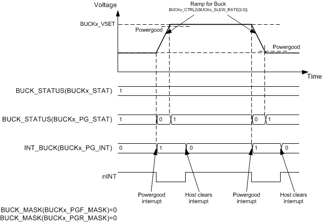
GUID-9E87B084-4FA9-4D5F-91FB-261535E3B1A1-low.gifFigure 7-6 Buck Output Voltage Change