SNVSBU3 March 2021 LP87702
PRODUCTION DATA
- 1 Features
- 2 Applications
- 3 Description
- 4 Revision History
- 5 Pin Configuration and Functions
- 6 Specifications
-
7 Detailed Description
- 7.1 Overview
- 7.2 Functional Block Diagram
- 7.3
Feature Descriptions
- 7.3.1 Step-Down DC/DC Converters
- 7.3.2 Boost Converter
- 7.3.3 Spread-Spectrum Mode
- 7.3.4 Sync Clock Functionality
- 7.3.5 Power-Up
- 7.3.6 Buck and Boost Control
- 7.3.7 Enable and Disable Sequences
- 7.3.8 Window Watchdog
- 7.3.9 Device Reset Scenarios
- 7.3.10 Diagnostics and Protection Features
- 7.3.11 OTP Error Correction
- 7.3.12 Operation of GPO Signals
- 7.3.13 Digital Signal Filtering
- 7.4 Device Functional Modes
- 7.5 Programming
- 7.6 Register Maps
- 8 Application and Implementation
- 9 Power Supply Recommendations
- 10Layout
- 11Device and Documentation Support
- 12Mechanical, Packaging, and Orderable Information
Package Options
Mechanical Data (Package|Pins)
- RHB|32
Thermal pad, mechanical data (Package|Pins)
- RHB|32
Orderable Information
7.3.10.3 Power-Good Information to Interrupt, PG0, and PG1 Pins
LP87702 supports both interrupt based indication of the power-good levels for various voltage settings and uses two power-good signals, PG0 and PG1. The selection of monitored signals is independent for the interrupt (nINT) and PG0 and PG1 signals. Each signal can include the following:
- The output voltage of one or both BUCKx converters
- The output voltage of the BOOST converter
- Input voltage of VANA
- Input voltage of VMON1 and VMON2 or both
- Thermal warning
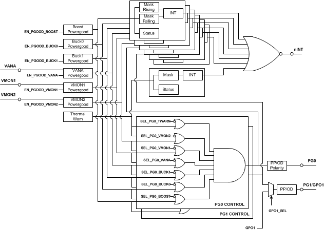
Figure 7-9 shows the block diagram for power-good connections to PG0 and PG1 pins and interrupt.
Monitored signals are enabled in the PGOOD_CTRL register. Converter output voltage monitoring (not current limit monitoring) can be selected for the indication. Monitoring is enabled by the EN_PGOOD_BUCKx and EN_PGOOD_BOOST bits. The monitoring is automatically masked to prevent it from forcing PGx inactive or causing an interrupt when a converter is disabled. Also, monitoring of VANA, VMON1, and VMON2 inputs can be independently enabled through the PGOOD_CTRL register. The type of voltage monitoring for the PGx signals and nINT is selected by the PGOOD_WINDOW bit. Only the undervoltage is monitored if the bit is 0 and the undervoltage and overvoltage are monitored if the bit is 1. See Section 7.3.10.1 for voltage monitoring thresholds.
Monitoring interrupts from all the output rails, input rails, and thermal warning are combined to the nINT pin. Dedicated mask bits are used to select which interrupts control the state of the nINT pin. See Table 7-5 for summary of the interrupts, mask bits, and interrupt clearing.
Similarly, enabled monitoring signals from all the output rails, input rails, and thermal warning are combined to PG0 and PG1 output pins. Register bits (SEL_PGx_x in PG0_CTRL and PG1_CTRL) select which of the signals control the state of PG0 and PG1, respectively. The polarity and the output type (push-pull or open-drain) of PG0 and PG1 are selected by the PGx_POL and PGx_OD bits in the PG_CTRL register.
PGx is only active or asserted when all monitored input voltages and all output voltages of the monitored and enabled converters are within the specified tolerance of the set target value.
PGx is inactive or de-asserted if any of the monitored input voltages or output voltages of the monitored and enabled converters are outside the specified tolerance of the set target value.
When PGx_RISE_DELAY = 1, PGx is set as active or asserted with 11 ms delay from the point of time where all the enabled power resource output voltages are within the specified tolerance for each requested or programmed output voltage.
Thermal shutdown and VANA overvoltage protection events force the PGx to the default state (the PGx are driven low, assuming the PGx polarity set in the OTP is active high).
 Figure 7-9 Block Diagram
of Power-Good Connections
Figure 7-9 Block Diagram
of Power-Good ConnectionsLP87702 power-good detection has two operating modes selected in the OTP: gated (that is, unusual) or continuous (that is, invalid) mode of operation. These modes are described in Section 7.3.10.3.1 and in Section 7.3.10.3.2.