SLLS732A October 2006 – November 2019 SN65LBC174A-EP
PRODUCTION DATA.
- 1Features
- 2Applications
- 3Description
- 4Revision History
- 5Description (continued)
- 6Device and Documentation Support
- 7Mechanical, Packaging, and Orderable Information
Package Options
Refer to the PDF data sheet for device specific package drawings
Mechanical Data (Package|Pins)
- DW|16
- DW|20
Thermal pad, mechanical data (Package|Pins)
Orderable Information
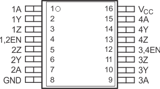
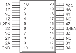
5.1 Pin Configuration and Functions
DW
16-Pin SOIC
Top View

DW
20-Pin SOIC
Top View

Pin Functions
| PIN | I/O | DESCRIPTION | ||
|---|---|---|---|---|
| NAME | 16 PINS | 20 PINS | ||
| 1A | 1 | 1 | Digital input | Port 1 A data input |
| 1Y | 2 | 2 | Bus output | Bus port 1 Y (complementary to 1 Z) |
| NC | — | 3 | No Connect | Physically not connected in package |
| 1Z | 3 | 4 | Bus output | Bus port 1 Z (complementary to 1 Y) |
| 1,2EN | 4 | 5 | Digital input | Bus output port 1 and 2 driver enable |
| 2Z | 5 | 6 | Bus output | Bus port 2 Z (complementary to 2 Y) |
| NC | — | 7 | No Connect | Physically not connected in package |
| 2Y | 6 | 8 | Bus output | Bus port 2 Y (complementary to 2 Z) |
| 2A | 7 | 9 | Digital input | Port 2 A data input |
| GND | 8 | 10 | Ground | Device ground |
| 3A | 9 | 11 | Digital input | Port 3 A data input |
| 3Y | 10 | 12 | Bus output | Bus port 3 Y (complementary to 3 Z) |
| NC | — | 13 | No Connect | Physically not connected in package |
| 3Z | 11 | 14 | Bus output | Bus port 3 Z (complementary to 3 Y) |
| 3,4EN | 12 | 15 | Digital input | Bus output port 3 and 4 driver enable |
| 4Z | 13 | 16 | Bus output | Bus port 4 Z (complementary to 4 Y) |
| NC | — | 17 | No Connect | Physically not connected in package |
| 4Y | 14 | 18 | Bus output | Bus port 4 Y (complementary to 4 Z) |
| 4A | 15 | 19 | Digital input | Port 4 A data input |
| VCC | 16 | 20 | VCC | Device power |