SLLS732A October   2006  – November 2019 SN65LBC174A-EP

PRODUCTION DATA.  

  1. 1Features
  2. 2Applications
  3. 3Description
    1.     Device Images
      1.      Logic Diagram (Positive Logic)
  4. 4Revision History
  5. 5Description (continued)
    1. 5.1 Pin Configuration and Functions
      1.      Pin Functions
    2. 5.2 Specifications
      1. 5.2.1 Absolute Maximum Ratings
      2. 5.2.2 ESD Ratings
      3. 5.2.3 Recommended Operating Conditions
      4. 5.2.4 Thermal Information
      5. 5.2.5 Electrical Characteristics
      6. 5.2.6 Switching Characteristics
      7. 5.2.7 Typical Characteristics
    3. 5.3 Parameter Measurement Information
    4. 5.4 Detailed Description
      1. 5.4.1 Overview
      2. 5.4.2 Functional Block Diagram
      3. 5.4.3 Feature Description
      4. 5.4.4 Device Functional Modes
    5. 5.5 Application and Implementation
      1. 5.5.1 Application Information
      2. 5.5.2 Typical Application
        1. 5.5.2.1 Design Requirements
        2. 5.5.2.2 Detailed Design Procedure
        3. 5.5.2.3 Application Curve
    6. 5.6 Power Supply Recommendations
    7. 5.7 Layout
      1. 5.7.1 Layout Guidelines
      2. 5.7.2 Layout Example
  6. 6Device and Documentation Support
    1. 6.1 Receiving Notification of Documentation Updates
    2. 6.2 Support Resources
    3. 6.3 Trademarks
    4. 6.4 Electrostatic Discharge Caution
    5. 6.5 Glossary
  7. 7Mechanical, Packaging, and Orderable Information

Package Options

Refer to the PDF data sheet for device specific package drawings

Mechanical Data (Package|Pins)
  • DW|16
  • DW|20
Thermal pad, mechanical data (Package|Pins)
Orderable Information

Typical Application

The following block diagram shows an MCU host connected via RS-485 to a SPI slave device. This device can be an ADC, DAC, MCU, or other SPI slave peripheral.
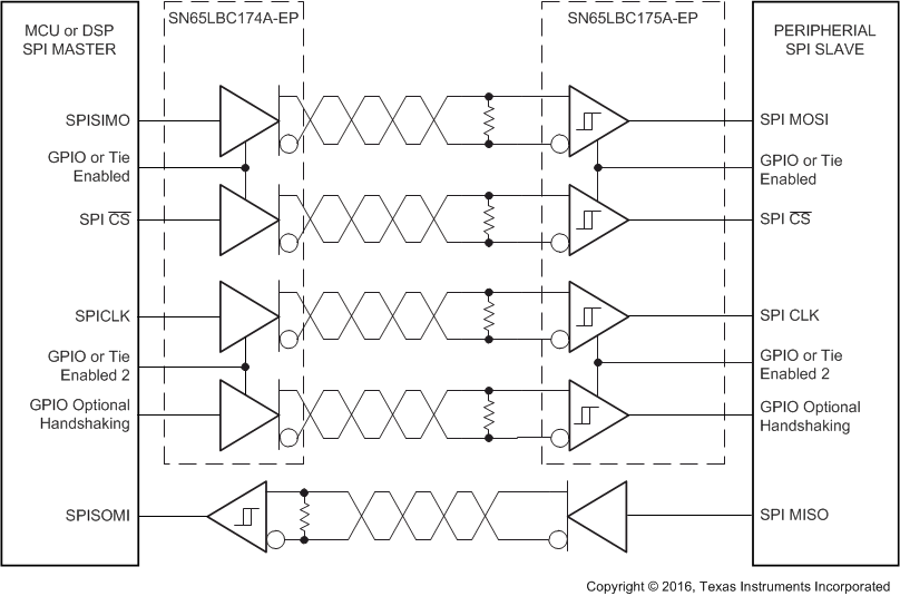
SN65LBC174A-EP fig011_typ_app_cir_sllseu5.gifFigure 16. Typical Application Circuit, MCU Master to Slave Link Via Serial Peripheral Interface