SLOS823D December 2012 – March 2020 THS4531A
PRODUCTION DATA.
- 1 Features
- 2 Applications
- 3 Description
- 4 Revision History
- 5 Related Products
- 6 Pin Configuration and Functions
- 7 Specifications
- 8 Detailed Description
-
9 Application and Implementation
- 9.1
Application Information
- 9.1.1 Frequency Response, and Output Impedance
- 9.1.2 Distortion
- 9.1.3 Slew Rate, Transient Response, Settling Time, Overdrive, Output Voltage, and Turnon and Turnoff Time
- 9.1.4 Common-Mode and Power Supply Rejection
- 9.1.5 VOCM Input
- 9.1.6 Balance Error
- 9.1.7 Single-Supply Operation
- 9.1.8 Low-Power Applications and the Effects of Resistor Values on Bandwidth
- 9.1.9 Driving Capacitive Loads
- 9.1.10 Audio Performance
- 9.1.11 Audio On and Off Pop Performance
- 9.2
Typical Applications
- 9.2.1 SAR ADC Performance: THS4531A and ADS8321 Combined Performance
- 9.2.2 Audio ADC Driver Performance: THS4531A and PCM4204 Combined Performance
- 9.2.3 SAR ADC Performance: THS4531A and ADS7945 Combined Performance
- 9.2.4 Differential-Input to Differential-Output Amplifier
- 9.2.5 Single-Ended to Differential FDA Configuration
- 9.2.6 Single-Ended Input to Differential Output Amplifier
- 9.2.7 Differential Input to Single-Ended Output Amplifier
- 9.1
Application Information
- 10Power Supply Recommendations
- 11Layout
- 12Device and Documentation Support
- 13Mechanical, Packaging, and Orderable Information
Package Options
Mechanical Data (Package|Pins)
Thermal pad, mechanical data (Package|Pins)
- RUN|10
Orderable Information
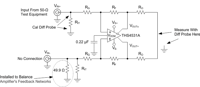
9.1.6 Balance Error
The circuit shown in Figure 75 is used to measure the balance error of the main differential amplifier. A network analyzer is used as the signal source and the measurement device. The output impedance of the network analyzer is 50 Ω and is DC coupled. RIT and RG are chosen to impedance match to 50 Ω and maintain the proper gain. To balance the amplifier, a 49.9-Ω resistor to ground is inserted across RIT on the alternate input. The output is measured using a high impedance differential probe at the summing junction of the two RO resistors, with respect to ground.
 Figure 75. Balance Error Test Circuit