SLOS823D December 2012 – March 2020 THS4531A
PRODUCTION DATA.
- 1 Features
- 2 Applications
- 3 Description
- 4 Revision History
- 5 Related Products
- 6 Pin Configuration and Functions
- 7 Specifications
- 8 Detailed Description
-
9 Application and Implementation
- 9.1
Application Information
- 9.1.1 Frequency Response, and Output Impedance
- 9.1.2 Distortion
- 9.1.3 Slew Rate, Transient Response, Settling Time, Overdrive, Output Voltage, and Turnon and Turnoff Time
- 9.1.4 Common-Mode and Power Supply Rejection
- 9.1.5 VOCM Input
- 9.1.6 Balance Error
- 9.1.7 Single-Supply Operation
- 9.1.8 Low-Power Applications and the Effects of Resistor Values on Bandwidth
- 9.1.9 Driving Capacitive Loads
- 9.1.10 Audio Performance
- 9.1.11 Audio On and Off Pop Performance
- 9.2
Typical Applications
- 9.2.1 SAR ADC Performance: THS4531A and ADS8321 Combined Performance
- 9.2.2 Audio ADC Driver Performance: THS4531A and PCM4204 Combined Performance
- 9.2.3 SAR ADC Performance: THS4531A and ADS7945 Combined Performance
- 9.2.4 Differential-Input to Differential-Output Amplifier
- 9.2.5 Single-Ended to Differential FDA Configuration
- 9.2.6 Single-Ended Input to Differential Output Amplifier
- 9.2.7 Differential Input to Single-Ended Output Amplifier
- 9.1
Application Information
- 10Power Supply Recommendations
- 11Layout
- 12Device and Documentation Support
- 13Mechanical, Packaging, and Orderable Information
Package Options
Mechanical Data (Package|Pins)
Thermal pad, mechanical data (Package|Pins)
- RUN|10
Orderable Information
8.3.2 Power Down
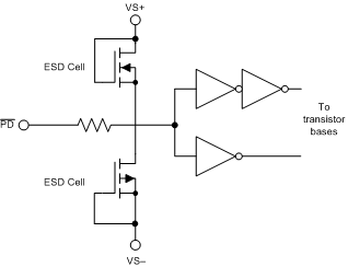
The power down pin is internally connected to a CMOS stage which must be driven to a minimum of 2.1 V to ensure proper high logic.
 Figure 68. Simplified Power-Down Internal Circuit
 If 1.8-V logic is used to drive the pin, a shoot through current of up to 100 µA may develop in the digital logic causing the overall quiescent current to exceed the 2 µA of maximum disabled quiescent current specified in the Electrical Characteristics: VS = 2.7 V.
To properly interface to 1.8-V logic with minimal increase in additional current draw, a logic-level translator like the SN74AVC1T45 device can be used.
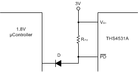
Alternatively, the same function can be achieved using a diode and pullup resistor as shown in Figure 69.
 Figure 69. THS4531A Power Down Interface to 1.8-V Logic Microcontroller
 The voltage at the power down pin will be a function of the supply voltage, input logic level, and diode drop. As long as the diode is forward biased, the power down voltage is calculated using Equation 3.

where
- VL is the logic level voltage.
- Vf is the forward voltage drop across the diode.
This means for 1.8-V logic, the forward voltage of the diode should be greater than 0.3 V but less than 0.7 V to keep the power down logic level above 2.1 V and less than 0.7 V respectively.
For example, if 1N914 is selected as the diode with a forward voltage of approximately 0.4 V, the translated logic voltages will be 0.4 V for disabled operation and 2.2 V for enabled operation.
Use Equation 4 to calculate the additional current draw.

Equation 2 shows that larger values of RPU result in a smaller additional current. A reasonable value of RPU is 500 kΩ where an additional current draw of 5.2 µA is expected while the device is in operation and 1.6 µA when disabled.