SLOS823D December 2012 – March 2020 THS4531A
PRODUCTION DATA.
- 1 Features
- 2 Applications
- 3 Description
- 4 Revision History
- 5 Related Products
- 6 Pin Configuration and Functions
- 7 Specifications
- 8 Detailed Description
-
9 Application and Implementation
- 9.1
Application Information
- 9.1.1 Frequency Response, and Output Impedance
- 9.1.2 Distortion
- 9.1.3 Slew Rate, Transient Response, Settling Time, Overdrive, Output Voltage, and Turnon and Turnoff Time
- 9.1.4 Common-Mode and Power Supply Rejection
- 9.1.5 VOCM Input
- 9.1.6 Balance Error
- 9.1.7 Single-Supply Operation
- 9.1.8 Low-Power Applications and the Effects of Resistor Values on Bandwidth
- 9.1.9 Driving Capacitive Loads
- 9.1.10 Audio Performance
- 9.1.11 Audio On and Off Pop Performance
- 9.2
Typical Applications
- 9.2.1 SAR ADC Performance: THS4531A and ADS8321 Combined Performance
- 9.2.2 Audio ADC Driver Performance: THS4531A and PCM4204 Combined Performance
- 9.2.3 SAR ADC Performance: THS4531A and ADS7945 Combined Performance
- 9.2.4 Differential-Input to Differential-Output Amplifier
- 9.2.5 Single-Ended to Differential FDA Configuration
- 9.2.6 Single-Ended Input to Differential Output Amplifier
- 9.2.7 Differential Input to Single-Ended Output Amplifier
- 9.1
Application Information
- 10Power Supply Recommendations
- 11Layout
- 12Device and Documentation Support
- 13Mechanical, Packaging, and Orderable Information
Package Options
Mechanical Data (Package|Pins)
Thermal pad, mechanical data (Package|Pins)
- RUN|10
Orderable Information
9.1.9 Driving Capacitive Loads
The THS4531A is designed for a nominal parasitic capacitive load of 2 pF (differentially). When driving capacitive loads greater than this, TI recommends using small resisters (RO) in series with the output as close to the device as possible. Without RO, capacitance on the output interacts with the output impedance of the amplifier causing phase shift in the loop gain of the amplifier that reduces the phase margin resulting in:
- Peaking in the frequency response.
- Overshoot, undershoot, and ringing in the time domain response with a pulse or square-wave signal.
- May lead to instability or oscillation.
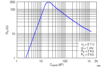
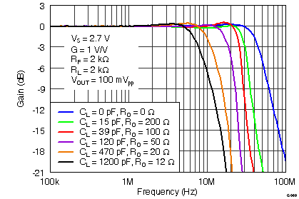
Inserting RO compensates the phase shift and restores the phase margin, but it also limits bandwidth. The circuit shown in Figure 71 is used to test for best RO versus capacitive loads, CL, with a capacitance placed differential across the VOUT+ and VOUT- along with 2-kΩ load resistor, and the output is measure with a differential probe. Figure 77 shows the suggested values of RO versus capacitive loads, CL, and Figure 78 shows the frequency response with various values. Performance is the same on both 2.7-V and 5-V supply.
 Figure 77. Recommended Series Output Resistor vs Capacitive Load for Flat Frequency Response
  Figure 78. Frequency Response for Various RO and CL Values