SLVS074I January 1983 – July 2022 TL494
PRODUCTION DATA
- 1 Features
- 2 Applications
- 3 Description
- 4 Simplified Block Diagram
- 5 Revision History
- 6 Pin Configuration and Functions
-
7 Specifications
- 7.1 Absolute Maximum Ratings
- 7.2 ESD Ratings
- 7.3 Recommended Operating Conditions
- 7.4 Thermal Information
- 7.5 Electrical Characteristics, Reference Section
- 7.6 Electrical Characteristics, Oscillator Section
- 7.7 Electrical Characteristics, Error-Amplifier Section
- 7.8 Electrical Characteristics, Output Section
- 7.9 Electrical Characteristics, Dead-Time Control Section
- 7.10 Electrical Characteristics, PWM Comparator Section
- 7.11 Electrical Characteristics, Total Device
- 7.12 Switching Characteristics
- 7.13 Typical Characteristics
- 8 Parameter Measurement Information
- 9 Detailed Description
- 10Application and Implementation
- 11Power Supply Recommendations
- 12Layout
- 13Device and Documentation Support
- 14Mechanical, Packaging, and Orderable Information
Package Options
Mechanical Data (Package|Pins)
Thermal pad, mechanical data (Package|Pins)
Orderable Information
7.6 Electrical Characteristics, Oscillator Section
CT = 0.01 μF, RT = 12 kΩ (see Figure 8-1)
| PARAMETER | TEST CONDITIONS(1) | TL494C, TL494I | UNIT | ||
|---|---|---|---|---|---|
| MIN | TYP(2) | MAX | |||
| Frequency | 10 | kHz | |||
| Standard deviation of frequency(3) | All values of VCC, CT, RT, and TA constant | 100 | Hz/kHz | ||
| Frequency change with voltage | VCC = 7 V to 40 V, TA = 25°C | 1 | Hz/kHz | ||
| Frequency change with temperature(4) | ΔTA = MIN to MAX | 10 | Hz/kHz | ||
(1) For conditions shown as MIN or MAX, use the appropriate value specified under recommended operating conditions.
(2) All typical values, except for parameter changes with temperature, are at TA = 25°C.
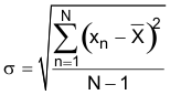
(3) Standard deviation is a measure of the statistical distribution about the mean as derived from the formula:
(4) Temperature coefficient of timing capacitor and timing resistor are not taken into account.