SLVS074I January 1983 – July 2022 TL494
PRODUCTION DATA
- 1 Features
- 2 Applications
- 3 Description
- 4 Simplified Block Diagram
- 5 Revision History
- 6 Pin Configuration and Functions
-
7 Specifications
- 7.1 Absolute Maximum Ratings
- 7.2 ESD Ratings
- 7.3 Recommended Operating Conditions
- 7.4 Thermal Information
- 7.5 Electrical Characteristics, Reference Section
- 7.6 Electrical Characteristics, Oscillator Section
- 7.7 Electrical Characteristics, Error-Amplifier Section
- 7.8 Electrical Characteristics, Output Section
- 7.9 Electrical Characteristics, Dead-Time Control Section
- 7.10 Electrical Characteristics, PWM Comparator Section
- 7.11 Electrical Characteristics, Total Device
- 7.12 Switching Characteristics
- 7.13 Typical Characteristics
- 8 Parameter Measurement Information
- 9 Detailed Description
- 10Application and Implementation
- 11Power Supply Recommendations
- 12Layout
- 13Device and Documentation Support
- 14Mechanical, Packaging, and Orderable Information
Package Options
Mechanical Data (Package|Pins)
Thermal pad, mechanical data (Package|Pins)
Orderable Information
10.2.2.5 Transistor Power-Switch Calculations
The transistor power switch was constructed with an NTE153 pnp drive transistor and an NTE331 npn output transistor. These two power devices were connected in a pnp hybrid Darlington circuit configuration (see Figure 10-7).
 Figure 10-7 Power-Switch Section
The hybrid Darlington circuit must be saturated at a maximum output current of IO + ΔIL/2 or 10.8 A. The Darlington hFE at 10.8 A must be high enough not to exceed the 250-mA maximum output collector current of the TL494. Based on published NTE153 and NTE331 specifications, the required power-switch minimum drive was calculated by Equation 16 through Equation 18 to be 144 mA:


The value of R10 was calculated by:
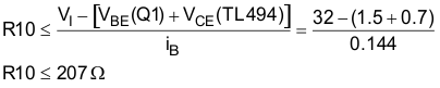
Based on these calculations, the nearest standard resistor value of 220 Ω was selected for R10. Resistors R11 and R12 permit the discharge of carriers in switching transistors when they are turned off.
The power supply described demonstrates the flexibility of the TL494 PWM control circuit. This power-supply design demonstrates many of the power-supply control methods provided by the TL494, as well as the versatility of the control circuit.