SLVS074I January 1983 – July 2022 TL494
PRODUCTION DATA
- 1 Features
- 2 Applications
- 3 Description
- 4 Simplified Block Diagram
- 5 Revision History
- 6 Pin Configuration and Functions
-
7 Specifications
- 7.1 Absolute Maximum Ratings
- 7.2 ESD Ratings
- 7.3 Recommended Operating Conditions
- 7.4 Thermal Information
- 7.5 Electrical Characteristics, Reference Section
- 7.6 Electrical Characteristics, Oscillator Section
- 7.7 Electrical Characteristics, Error-Amplifier Section
- 7.8 Electrical Characteristics, Output Section
- 7.9 Electrical Characteristics, Dead-Time Control Section
- 7.10 Electrical Characteristics, PWM Comparator Section
- 7.11 Electrical Characteristics, Total Device
- 7.12 Switching Characteristics
- 7.13 Typical Characteristics
- 8 Parameter Measurement Information
- 9 Detailed Description
- 10Application and Implementation
- 11Power Supply Recommendations
- 12Layout
- 13Device and Documentation Support
- 14Mechanical, Packaging, and Orderable Information
Package Options
Mechanical Data (Package|Pins)
Thermal pad, mechanical data (Package|Pins)
Orderable Information
10.2.2.4 Output Capacitance Calculations
Once the filter inductor has been calculated, the value of the output filter capacitor is calculated to meet the output ripple requirements. An electrolytic capacitor can be modeled as a series connection of an inductance, a resistance, and a capacitance. To provide good filtering, the ripple frequency must be far below the frequencies at which the series inductance becomes important. So, the two components of interest are the capacitance and the effective series resistance (ESR). The maximum ESR is calculated according to the relation between the specified peak-to-peak ripple voltage and the peak-to-peak ripple current.
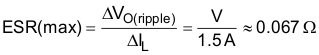
The minimum capacitance of C3 necessary to maintain the VO ripple voltage at less than the 100-mV design objective is calculated according to Equation 15:
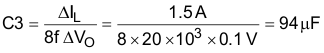
A 220-mF, 60-V capacitor is selected because it has a maximum ESR of 0.074 Ω and a maximum ripple current of 2.8 A.