SLVS568E January 2005 – July 2025 TLV341 , TLV341A , TLV342 , TLV342S
PRODUCTION DATA
- 1
- 1 Features
- 2 Applications
- 3 Description
- 4 Pin Configuration and Functions
-
5 Specifications
- 5.1 Absolute Maximum Ratings
- 5.2 ESD Ratings
- 5.3 Recommended Operating Conditions
- 5.4 Thermal Information: TLV341
- 5.5 Thermal Information: TLV342
- 5.6 Thermal Information: TLV342S
- 5.7 Electrical Characteristics: V+ = 1.8V
- 5.8 Electrical Characteristics: V+ = 5V
- 5.9 Shutdown Characteristics: V+ = 1.8V
- 5.10 Shutdown Characteristics: V+ = 5V
- 5.11 Typical Characteristics
- 6 Detailed Description
- 7 Application and Implementation
- 8 Device and Documentation Support
- 9 Revision History
- 10Mechanical, Packaging, and Orderable Information
Package Options
Mechanical Data (Package|Pins)
Thermal pad, mechanical data (Package|Pins)
Orderable Information
4 Pin Configuration and Functions
 Figure 4-1 TLV341 DBV or DCK Package,6-Pin SOT-23 or SC70(Top View)
 Figure 4-2 TLV341 DRL Package,6-Pin SOT(Top View)
Table 4-1 Pin Functions: TLV341
| PIN | I/O | DESCRIPTION | ||
|---|---|---|---|---|
| NAME | SOT-23, SC70 | SOT | ||
| 1IN+ | 1 | 2 | I | Noninverting input on channel 1 |
| 1IN– | 3 | 3 | I | Inverting input on channel 1 |
| 1OUT | 4 | 4 | O | Output on channel 1 |
| GND | 2 | 1 | — | Ground |
| SHDN | 5 | 5 | I | Shutdown active low |
| V+ | 6 | 6 | — | Positive power supply |
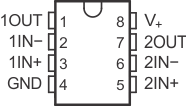
 Figure 4-3 TLV342 D or DGK Package,10-Pin SOIC or VSSOP(Top View)
 Figure 4-4 TLV342 RUG Package,10-Pin X2QFN(Top View)
Table 4-2 Pin Functions: TLV342
| PIN | I/O | DESCRIPTION | ||
|---|---|---|---|---|
| NAME | SOIC, VSSOP | X2QFN | ||
| 1IN+ | 3 | 1 | I | Noninverting input on channel 1 |
| 1IN– | 2 | 10 | I | Inverting input on channel 1 |
| 1OUT | 1 | 9 | O | Output on channel 1 |
| 2IN+ | 5 | 4 | I | Noninverting input on channel 2 |
| 2IN– | 6 | 5 | I | Inverting input on channel 2 |
| 2OUT | 7 | 6 | O | Output on channel 2 |
| GND | 4 | 2 | — | Ground |
| NC(1) | — | 3, 8 | — | Not connected |
| V+ | 8 | 7 | — | Positive power supply |
(1) NC – No internal connection
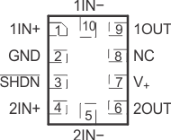
 Figure 4-5 TLV342S RUG Package,10-Pin
X2QFN(Top View)
Figure 4-5 TLV342S RUG Package,10-Pin
X2QFN(Top View)Table 4-3 Pin Functions: TLV342S
| PIN | I/O | DESCRIPTION | |
|---|---|---|---|
| NAME | NO. | ||
| 1IN+ | 1 | I | Noninverting input on channel 1 |
| 1IN– | 10 | I | Inverting input on channel 1 |
| 1OUT | 9 | O | Output on channel 1 |
| 2IN+ | 4 | I | Noninverting input on channel 2 |
| 2IN– | 5 | I | Inverting input on channel 2 |
| 2OUT | 6 | O | Output on channel 2 |
| GND | 2 | — | Ground |
| NC(1) | 8 | — | Not connected |
| SHDN | 3 | I | Shutdown active low |
| V+ | 7 | — | Positive power supply |
(1) NC – No internal connection