SLVS568E January 2005 – July 2025 TLV341 , TLV341A , TLV342 , TLV342S
PRODUCTION DATA
- 1
- 1 Features
- 2 Applications
- 3 Description
- 4 Pin Configuration and Functions
-
5 Specifications
- 5.1 Absolute Maximum Ratings
- 5.2 ESD Ratings
- 5.3 Recommended Operating Conditions
- 5.4 Thermal Information: TLV341
- 5.5 Thermal Information: TLV342
- 5.6 Thermal Information: TLV342S
- 5.7 Electrical Characteristics: V+ = 1.8V
- 5.8 Electrical Characteristics: V+ = 5V
- 5.9 Shutdown Characteristics: V+ = 1.8V
- 5.10 Shutdown Characteristics: V+ = 5V
- 5.11 Typical Characteristics
- 6 Detailed Description
- 7 Application and Implementation
- 8 Device and Documentation Support
- 9 Revision History
- 10Mechanical, Packaging, and Orderable Information
Package Options
Mechanical Data (Package|Pins)
Thermal pad, mechanical data (Package|Pins)
Orderable Information
5.11 Typical Characteristics
 Figure 5-1 Supply Current vs
Supply Voltage
 Figure 5-3 Output Voltage Swing vs
Supply Voltage
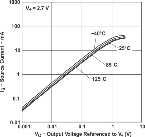 Figure 5-5 Source Current vs
Output Voltage
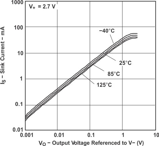 Figure 5-7 Sink Current vs
Output Voltage
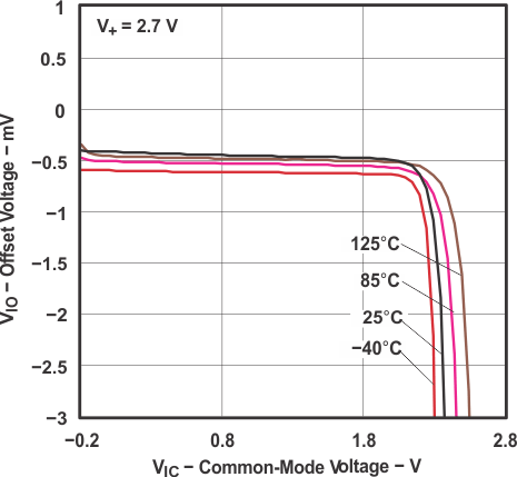 Figure 5-9 Offset Voltage vs
Common-Mode Voltage
 Figure 5-11 Input Voltage vs Output Voltage
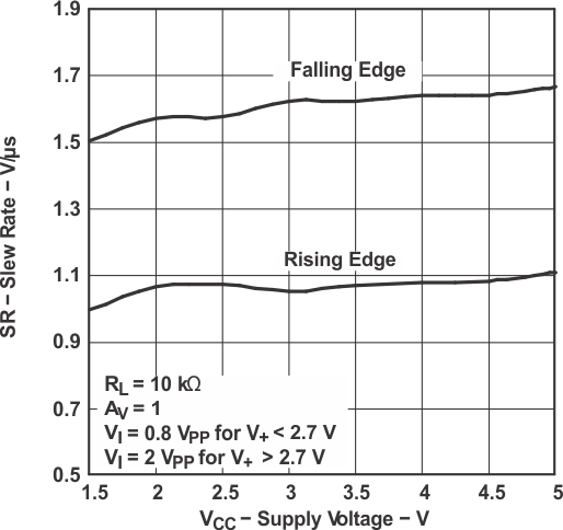 Figure 5-13 Slew Rate vs
Supply Voltage
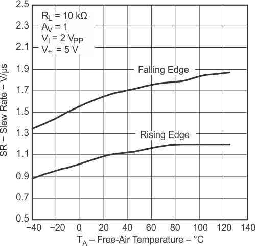 Figure 5-15 Slew Rate vs
Temperature
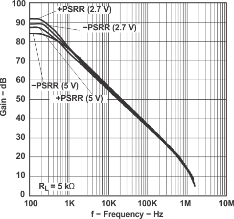 Figure 5-17 PSRR vs Frequency
 Figure 5-19 Total Harmonic Distortion +Noise
 vs Frequency
 Figure 5-21 Frequency Response vs
Temperature
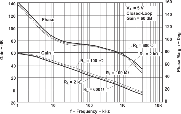 Figure 5-23 Frequency Response vs RL
 Figure 5-25 Small-Signal Noninverting Response
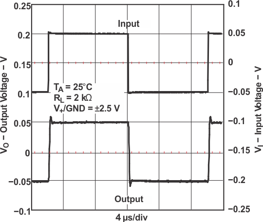 Figure 5-27 Small-Signal Noninverting Response
 Figure 5-29 Small-Signal Noninverting Response
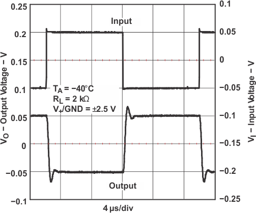 Figure 5-31 Small-Signal Noninverting Response
 Figure 5-33 Small-Signal Inverting Response
 Figure 5-35 Small-Signal Inverting Response
 Figure 5-2 Input Bias Current vs
Temperature
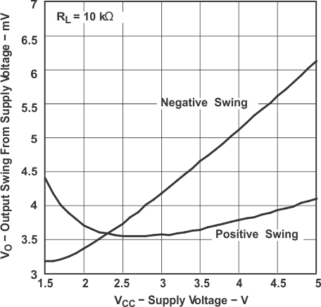 Figure 5-4 Output Voltage Swing vs
Supply Voltage
 Figure 5-6 Source Current vs
Output Voltage
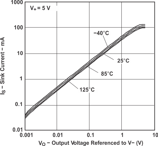 Figure 5-8 Sink Current vs
Output Voltage
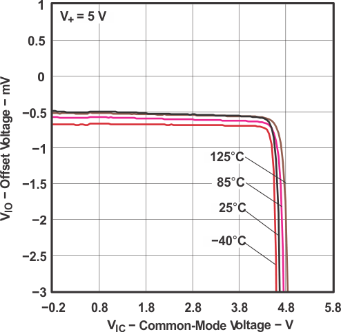 Figure 5-10 Offset Voltage vs
Common-Mode Voltage
 Figure 5-12 Input Voltage vs
Output Voltage
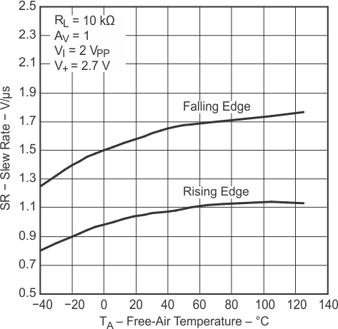 Figure 5-14 Slew Rate vs
Temperature
 Figure 5-16 CMRR vs Frequency
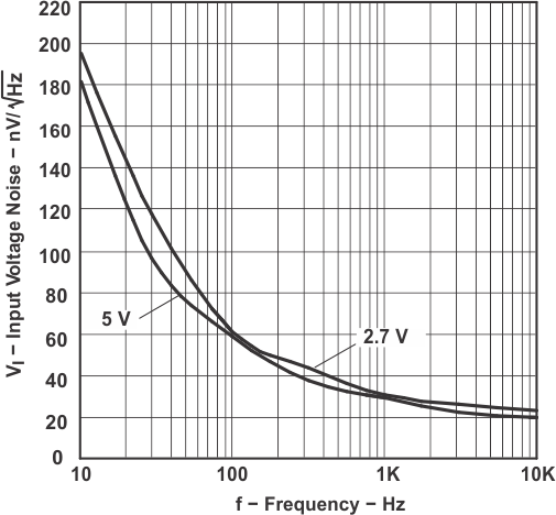 Figure 5-18 Input Voltage Noise vs
Frequency
 Figure 5-20 Total Harmonic Distortion +Noise
 vs Output Voltage
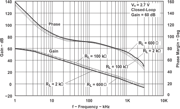 Figure 5-22 Frequency Response vs RL
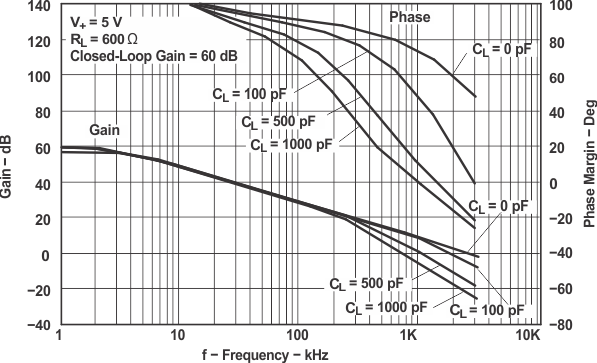 Figure 5-24 Frequency Response vs CL
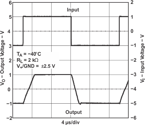 Figure 5-26 Large-Signal Noninverting Response
 Figure 5-28 Large-Signal Noninverting Response
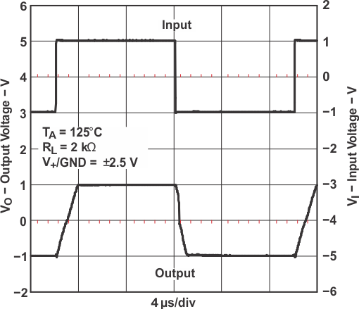 Figure 5-30 Large-Signal Noninverting Response
 Figure 5-32 Large-Signal Inverting Response
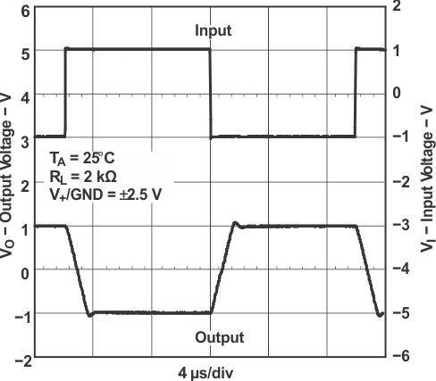 Figure 5-34 Large-Signal Inverting Response
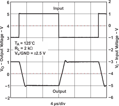 Figure 5-36 Large-Signal Inverting Response