SLVSFQ6A November 2020 – June 2021 TPS2640
PRODUCTION DATA
- 1 Features
- 2 Applications
- 3 Description
- 4 Revision History
- 5 Device Comparison
- 6 Pin Configuration and Functions
- 7 Specifications
- 8 Parameter Measurement Information
-
9 Detailed Description
- 9.1 Overview
- 9.2 Functional Block Diagram
- 9.3
Feature Description
- 9.3.1 Undervoltage Lockout (UVLO)
- 9.3.2 Overvoltage Protection (OVP)
- 9.3.3 Reverse Input Supply Protection
- 9.3.4 Hot Plug-In and In-Rush Current Control
- 9.3.5 Overload and Short Circuit Protection
- 9.4 Device Functional Modes
-
10Application and Implementation
- 10.1 Application Information
- 10.2 Typical Application
- 10.3 System Examples
- 10.4 Do's and Dont's
- 11Power Supply Recommendations
- 12Layout
- 13Device and Documentation Support
- 14Mechanical, Packaging, and Orderable Information
Package Options
Mechanical Data (Package|Pins)
Thermal pad, mechanical data (Package|Pins)
- PWP|16
Orderable Information
11.1 Transient Protection
In case of short circuit and over load current limit, when the device interrupts current flow, input inductance generates a positive voltage spike on the input and output inductance generates a negative voltage spike on the output. The peak amplitude of voltage spikes (transients) is dependent on value of inductance in series to the input or output of the device. Such transients can exceed the Abolsute Maximum Ratings of the device if steps are not taken to address the issue.
Typical methods for addressing transients include
- Minimizing lead length and inductance into and out of the device
- Using large PCB GND plane
- Schottky diode across the output to absorb negative spikes
- A low value ceramic capacitor (C(IN) to approximately 0.1 μF) to absorb the energy and dampen the transients.
The approximate value of input capacitance can be estimated with Equation 24.
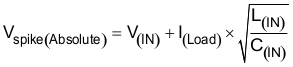
where
- V(IN) is the nominal supply voltage
- I(LOAD) is the load current
- L(IN) equals the effective inductance seen looking into the source
- C(IN) is the capacitance present at the input
Some applications may require additional Transient Voltage Suppressor (TVS) to prevent transients from exceeding the Abolsute Maximum Ratings of the device. These transients can occur during positive and negative surge tests on the supply lines. In such applications it is recommended to place atleast 1 μF of input capacitor to limit the falling slew rate of the input voltage within a maximum of 15 V/μs.
The circuit implementation with optional protection components (a ceramic capacitor, TVS and schottky diode) is shown in Figure 11-1.
